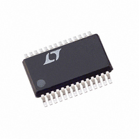
LTC1628IG-SYNC#PBF Linear Technology, LTC1628IG-SYNC#PBF Datasheet - Page 15

LTC1628IG-SYNC#PBF
Manufacturer Part Number
LTC1628IG-SYNC#PBF
Description
IC SW REG STEP-DOWN 28-SSOP
Manufacturer
Linear Technology
Type
Step-Down (Buck)r
Datasheet
1.LTC1628CG-SYNCPBF.pdf
(32 pages)
Specifications of LTC1628IG-SYNC#PBF
Internal Switch(s)
No
Synchronous Rectifier
Yes
Number Of Outputs
2
Voltage - Output
Adj to 0.8V
Current - Output
3A
Frequency - Switching
140kHz ~ 310kHz
Voltage - Input
3.5 ~ 30 V
Operating Temperature
-40°C ~ 85°C
Mounting Type
Surface Mount
Package / Case
28-SSOP
Lead Free Status / RoHS Status
Lead free / RoHS Compliant
Power - Output
-
Available stocks
Company
Part Number
Manufacturer
Quantity
Price
APPLICATIO S I FOR ATIO
synchronous MOSFET losses are greatest at high input
voltage when the top switch duty factor is low or during a
short-circuit when the synchronous switch is on close to
100% of the period.
The term (1+δ) is generally given for a MOSFET in the form
of a normalized R
δ = 0.005/°C can be used as an approximation for low
voltage MOSFETs. C
FET characteristics. The constant k = 1.7 can be used to
estimate the contributions of the two terms in the main
switch dissipation equation.
The Schottky diode D1 shown in Figure 1 conducts during
the dead-time between the conduction of the two power
MOSFETs. This prevents the body diode of the bottom
MOSFET from turning on, storing charge during the dead-
time and requiring a reverse recovery period that could
cost as much as 3% in efficiency at high V
Schottky is generally a good compromise for both regions
of operation due to the relatively small average current.
Larger diodes result in additional transition losses due to
their larger junction capacitance. Schottky diodes should
be placed in parallel with the synchronous MOSFETs when
operating in pulse-skip or in Burst Mode Operation.
C
The selection of C
tecture and its impact on the worst-case RMS current
drawn through the input network (battery/fuse/capacitor).
It can be shown that the worst case RMS current occurs
when only one controller is operating. The controller with
the highest (V
formula below to determine the maximum RMS current
requirement. Increasing the output current, drawn from
the other out-of-phase controller, will actually decrease
the input RMS ripple current from this maximum value
(see Figure 4). The out-of-phase technique typically re-
duces the input capacitor’s RMS ripple current by a factor
of 30% to 70% when compared to a single phase power
supply solution.
The type of input capacitor, value and ESR rating have
efficiency effects that need to be considered in the selec-
tion process. The capacitance value chosen should be
sufficient to store adequate charge to keep high peak
IN
and C
OUT
Selection
OUT
IN
)(I
U
DS(ON)
is simplified by the multiphase archi-
OUT
RSS
) product needs to be used in the
is usually specified in the MOS-
U
vs Temperature curve, but
W
IN
. A 1A to 3A
U
battery currents down. 20µF to 40µF is usually sufficient
for a 25W output supply operating at 200kHz. The ESR of
the capacitor is important for capacitor power dissipation
as well as overall battery efficiency. All of the power (RMS
ripple current • ESR) not only heats up the capacitor but
wastes power from the battery.
Medium voltage (20V to 35V) ceramic, tantalum, OS-CON
and switcher-rated electrolytic capacitors can be used as
input capacitors, but each has drawbacks: ceramic voltage
coefficients are very high and may have audible piezoelec-
tric effects; tantalums need to be surge-rated; OS-CONs
suffer from higher inductance, larger case size and limited
surface-mount applicability; electrolytics’ higher ESR and
dryout possibility require several to be used. Multiphase
systems allow the lowest amount of capacitance overall.
As little as one 22µF or two to three 10µF ceramic capaci-
tors are an ideal choice in a 20W to 35W power supply due
to their extremely low ESR. Even though the capacitance
at 20V is substantially below their rating at zero-bias, very
low ESR loss makes ceramics an ideal candidate for
highest efficiency battery operated systems. Also con-
sider parallel ceramic and high quality electrolytic capaci-
tors as an effective means of achieving ESR and bulk
capacitance goals.
In continuous mode, the source current of the top N-chan-
nel MOSFET is a square wave of duty cycle V
prevent large voltage transients, a low ESR input capacitor
sized for the maximum RMS current of one channel
mustbe used. The maximum RMS capacitor current is
given by:
This formula has a maximum at V
I
monly used for design because even significant devia-
tions do not offer much relief. Note that capacitor
manufacturer’s ripple current ratings are often based on
only 2000 hours of life. This makes it advisable to further
derate the capacitor, or to choose a capacitor rated at a
higher temperature than required. Several capacitors may
also be paralleled to meet size or height requirements in
RMS
C
IN
= I
Re
OUT
quiredI
/2. This simple worst case condition is com-
RMS
≈
I
MAX
LTC1628-SYNC
[
V
OUT
(
V
IN
IN
V
= 2V
−
IN
V
OUT
OUT
OUT
)
, where
/V
]
15
1 2
1628syncfa
/
IN
. To


