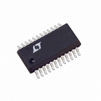
LTC1702IGN#TR Linear Technology, LTC1702IGN#TR Datasheet - Page 30

LTC1702IGN#TR
Manufacturer Part Number
LTC1702IGN#TR
Description
IC REG SW DUAL SYNC 2PH 24SSOP
Manufacturer
Linear Technology
Series
PolyPhase®r
Type
Step-Down (Buck)r
Datasheet
1.LTC1702CGN.pdf
(36 pages)
Specifications of LTC1702IGN#TR
Internal Switch(s)
No
Synchronous Rectifier
Yes
Number Of Outputs
2
Current - Output
1A, 25A
Frequency - Switching
550kHz
Voltage - Input
3 ~ 7 V
Operating Temperature
-40°C ~ 85°C
Mounting Type
Surface Mount
Package / Case
24-SSOP
Lead Free Status / RoHS Status
Contains lead / RoHS non-compliant
Voltage - Output
-
Power - Output
-
Available stocks
Company
Part Number
Manufacturer
Quantity
Price
APPLICATIONS
Making L smaller than this optimum value yields little or no
improvement in transient response. As the output voltage
recovers, the inductor current will briefly rise above the
level of the output current to replenish the charge lost from
the output capacitor. With a properly compensated loop,
the entire recovery time will be inside of 10µs.
Most loads care only about the maximum deviation from
ideal, which occurs somewhere in the first two cycles after
the load step hits. During this time, the output capacitor
does all the work until the inductor and control loop regain
control. The initial drop (or rise if the load steps down) is
entirely controlled by the ESR of the capacitor and amounts
to most of the total voltage drop. To minimize this drop,
reduce the ESR as much as possible by choosing low ESR
capacitors and/or paralleling multiple capacitors at the
output. The capacitance value accounts for the rest of the
voltage drop until the inductor current rises. With most
output capacitors, several devices paralleled to get the
ESR down will have so much capacitance that this drop
term is negligible. Ceramic capacitors are an exception; a
small ceramic capacitor can have suitably low ESR with
relatively small values of capacitance, making this second
drop term significant.
LTC1702
30
Figure 17c. Voltage Positioning Regulator
LTC1702
Figure 17a. Standard Regulator
LTC1702
FB
FB
U
INFORMATION
V
V
U
IN
IN
W
1702 F17a
V
OUT
1702 F17c
V
OUT
U
CURRENT
CURRENT
Figure 17b. Standard Regulator—Transient Response
Figure 17d. Positioning Regulator—Transient Response
LOAD
LOAD
V
V
Optimizing Loop Compensation
Loop compensation has a fundamental impact on tran-
sient recovery time, the time it takes the LTC1702 to
recover after the output voltage has dropped due to output
capacitor ESR. Optimizing loop compensation entails
maintaining the highest possible loop bandwidth while
ensuring loop stability. The Feedback Component Selec-
tion section describes in detail how to design an optimized
feedback loop, appropriate for most LTC1702 systems.
Voltage Positioning
If the load transients consist primarily of load steps from
near zero load to full load and back, the transient response
can be traded off against DC regulation performance by
using a technique known as “voltage positioning.” The
goal is to intentionally compromise the DC regulation loop
such that the output rides near the maximum allowable
value (often +5%) with no load and near the minimum
allowable value at maximum load. With the load at zero,
any transient that comes along will be a current increase
which will cause the output voltage to fall. Since the output
voltage is initially at a high value, it can fall further before
OUT
OUT
NOM
NOM
+5%
–5%
MAX
+5%
–5%
MAX
0
0
1702 F17b
1702 F17d
MAXIMUM
ALLOWABLE
TRANSIENT
MAXIMUM
ALLOWABLE
TRANSIENT
≈2× FIGURE 17b
1702fa


