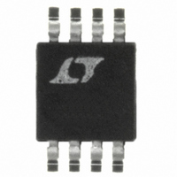
LT1614CMS8 Linear Technology, LT1614CMS8 Datasheet - Page 7

LT1614CMS8
Manufacturer Part Number
LT1614CMS8
Description
IC SW REG INVERTING 600KHZ 8MSOP
Manufacturer
Linear Technology
Type
Invertingr
Datasheet
1.LT1614CS8PBF.pdf
(16 pages)
Specifications of LT1614CMS8
Internal Switch(s)
Yes
Synchronous Rectifier
No
Number Of Outputs
1
Voltage - Output
Adj to -24V
Current - Output
500mA
Frequency - Switching
600kHz
Voltage - Input
0.92 ~ 5 V
Operating Temperature
0°C ~ 70°C
Mounting Type
Surface Mount
Package / Case
8-MSOP, Micro8™, 8-uMAX, 8-uSOP,
Lead Free Status / RoHS Status
Contains lead / RoHS non-compliant
Power - Output
-
Available stocks
Company
Part Number
Manufacturer
Quantity
Price
Company:
Part Number:
LT1614CMS8
Manufacturer:
LT
Quantity:
5 321
Part Number:
LT1614CMS8
Manufacturer:
LINEAR/凌特
Quantity:
20 000
Part Number:
LT1614CMS8#PBF
Manufacturer:
LINEAR/凌特
Quantity:
20 000
Company:
Part Number:
LT1614CMS8#TR
Manufacturer:
LT
Quantity:
24
Part Number:
LT1614CMS8#TRPBF
Manufacturer:
LINEAR/凌特
Quantity:
20 000
OPERATIO
When Q1 turns off during the second phase of switching,
the SWX node voltage abruptly increases to (V
The SW node voltage increases to V
current in the first loop, begining at C1, flows through L1,
C2, D1 and back to C1. Current in the second loop flows
from C3 through L2, D1 and back to C3. Load current
continues to be supplied by L2 and C3.
An important layout issue arises due to the chopped
nature of the currents flowing in Q1 and D1. If they are both
tied directly to the ground plane before being combined,
switching noise will be introduced into the ground plane.
It is almost impossible to get rid of this noise, once present
in the ground plane. The solution is to tie D1’s cathode to
the ground pin of the LT1614 before the combined cur-
V
V
IN
IN
+
+
U
Figure 6. Switch-Off Phase of Inverting Converter. L1 and L2 Current Have Negative dI/dt
C1
C1
Figure 5. Switch-On Phase of Inverting Converter. L1 and L2 Current Have Positive dI/dt
L1
L1
V
IN
D
+ V
V
(about 350mV). Now
CESAT
OUT
Q1
Q1
+ V
SW
SW
D
IN
–(V
+ |V
C2
C2
IN
+ V
OUT
V
D
OUT
SWX
SWX
|).
)
D1
D1
rents are dumped into the ground plane as drawn in
Figures 4, 5 and 6. This single layout technique can
virtually eliminate high frequency “spike” noise so often
present on switching regulator outputs.
Output ripple voltage appears as a triangular waveform
riding on V
of L2 multiplied by the equivalent series resistance (ESR)
of output capacitor C3. Increasing the inductance of L1
and L2 lowers the ripple current, which leads to lower
output voltage ripple. Decreasing the ESR of C3, by using
ceramic or other low ESR type capacitors, lowers output
ripple voltage. Output ripple voltage can be reduced to
arbitrarily low levels by using large value inductors and
low ESR, high value capacitors.
L2
L2
OUT
. Ripple magnitude equals the ripple current
+
+
C3
C3
1614 F06
1614 F05
R
R
LOAD
LOAD
–V
–V
OUT
OUT
LT1614
7


