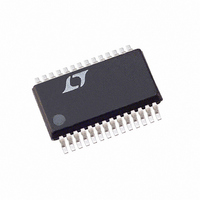
LTC1628CG-PG Linear Technology, LTC1628CG-PG Datasheet - Page 8

LTC1628CG-PG
Manufacturer Part Number
LTC1628CG-PG
Description
IC REG SW 2PHASE STEPDOWN 28SSOP
Manufacturer
Linear Technology
Type
Step-Down (Buck)r
Datasheet
1.LTC1628CGPBF.pdf
(32 pages)
Specifications of LTC1628CG-PG
Internal Switch(s)
No
Synchronous Rectifier
Yes
Number Of Outputs
2
Voltage - Output
Adj to 0.8V
Current - Output
3A
Frequency - Switching
220kHz
Voltage - Input
3.5 ~ 30 V
Operating Temperature
0°C ~ 85°C
Mounting Type
Surface Mount
Package / Case
28-SSOP
Lead Free Status / RoHS Status
Contains lead / RoHS non-compliant
Power - Output
-
Available stocks
Company
Part Number
Manufacturer
Quantity
Price
Company:
Part Number:
LTC1628CG-PG
Manufacturer:
LT
Quantity:
2 000
Part Number:
LTC1628CG-PG
Manufacturer:
LT/凌特
Quantity:
20 000
Part Number:
LTC1628CG-PG#PBF
Manufacturer:
LINEAR/凌特
Quantity:
20 000
Part Number:
LTC1628CG-PGTRPBF
Manufacturer:
LT/凌特
Quantity:
20 000
LTC1628/LTC1628-PG
PI FU CTIO S
RUN/SS1, RUN/SS2: Combination of soft-start, run con-
trol inputs and short-circuit detection timers. A capacitor
to ground at each of these pins sets the ramp time to full
output current. Forcing either of these pins back below
1.0V causes the IC to shut down the circuitry required for
that particular controller. Latchoff overcurrent protection
is also invoked via this pin as described in the Applications
Information section.
SENSE1
Current Comparators. The I
offsets between the SENSE
tion with R
SENSE1
Current Comparators.
V
back voltage for each controller from an external resistive
divider across the output.
FREQSET: Frequency Control Input to the Oscillator. This
pin can be left open, tied to ground, tied to INTV
by an external voltage source. This pin can also be used
with an external phase detector to build a true phase-
locked loop.
STBYMD: Control pin that determines which circuitry re-
mains active when the controllers are shut down and/or
provides a common control point to shut down both con-
trollers. See the Operation section for details.
FCB: Forced Continuous Control Input. This input acts on
the first controller (or both controllers depending upon
the FLTCPL pin—see pin description), and is
normally used to regulate a secondary winding. Pulling
this pin below 0.8V will force continuous synchronous
operation for the first and optionally the second control-
ler. Do not leave this pin floating.
I
Compensation Point. Each associated channels’ current
comparator trip point increases with this control voltage.
SGND: Small Signal Ground common to both con-
trollers, must be routed separately from high current
grounds to the common (–) terminals of the C
capacitors.
8
TH1,
OSENSE1
U
I
TH2
+
–
: Error Amplifier Output and Switching Regulator
, SENSE2
, SENSE2
, V
U
SENSE
OSENSE2
set the current trip threshold.
+
–
: Receives the remotely-sensed feed-
U
: The (+) Input to the Differential
: The (–) Input to the Differential
–
th
and SENSE
pin voltage and controlled
+
pins in conjunc-
CC
or driven
OUT
3.3V
10mA DC with peak currents as high as 50mA.
PGND: Driver Power Ground. Connects to the sources of
bottom (synchronous) N-channel MOSFETs, anodes of the
Schottky rectifiers and the (–) terminal(s) of C
INTV
Regulator and the EXTV
circuits are powered from this voltage source. Must be
decoupled to power ground with a minimum of 4.7 F tanta-
lum or other low ESR capacitor. The INTV
standby function is determined by the STBYMD pin.
EXTV
nected to INTV
power, bypassing the internal low dropout regulator, when-
ever EXTV
in Applications section. Do not exceed 7V on this pin.
BG1, BG2: High Current Gate Drives for Bottom (Synchro-
nous) N-Channel MOSFETs. Voltage swing at these pins is
from ground to INTV
V
between this pin and the signal ground pin.
BOOST1, BOOST2: Bootstrapped Supplies to the Top Side
Floating Drivers. Capacitors are connected between the
boost and switch pins and Schottky diodes are tied be-
tween the boost and INTV
boost pins is from INTV
SW1, SW2: Switch Node Connections to Inductors. Volt-
age swing at these pins is from a Schottky diode (external)
voltage drop below ground to V
TG1, TG2: High Current Gate Drives for Top N-Channel
MOSFETs. These are the outputs of floating drivers with a
voltage swing equal to INTV
the switch node voltage SW.
FLTCPL: (LTC1628 Only) Fault Coupling Control Pin that
determines if fault/normal conditions on one controller
will act on the other controller. FLTCPL = INTV
channels; FLTCPL = 0V to decouple.
IN
: Main Supply Pin. A bypass capacitor should be tied
CC
OUT
CC
: Output of the Internal 5V Linear Low Dropout
: External Power Input to an Internal Switch Con-
: Output of a linear regulator capable of supplying
CC
is higher than 4.7V. See EXTV
CC
. This switch closes and supplies V
CC
.
CC
CC
Switch. The driver and control
CC
to (V
CC
pins. Voltage swing at the
– 0.5V superimposed on
IN
IN
.
+ INTV
CC
CC
IN
).
CC
CC
connection
.
to couple
regulator
1628fb
CC


