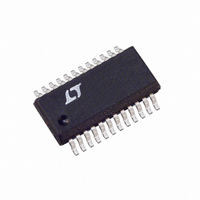
LTC3736EGN Linear Technology, LTC3736EGN Datasheet - Page 22

LTC3736EGN
Manufacturer Part Number
LTC3736EGN
Description
IC CTRLR SW SYNC DUAL 2PH 24SSOP
Manufacturer
Linear Technology
Series
PolyPhase®r
Type
Step-Down (Buck)r
Datasheet
1.LTC3736EGNPBF.pdf
(28 pages)
Specifications of LTC3736EGN
Internal Switch(s)
No
Synchronous Rectifier
Yes
Number Of Outputs
2
Voltage - Output
0.6 ~ 9.8 V
Current - Output
1A
Frequency - Switching
550kHz ~ 750kHz
Voltage - Input
2.75 ~ 9.8 V
Operating Temperature
-40°C ~ 85°C
Mounting Type
Surface Mount
Package / Case
24-SSOP
Lead Free Status / RoHS Status
Contains lead / RoHS non-compliant
Power - Output
-
Available stocks
Company
Part Number
Manufacturer
Quantity
Price
Company:
Part Number:
LTC3736EGN
Manufacturer:
Linear Technology
Quantity:
135
Company:
Part Number:
LTC3736EGN
Manufacturer:
ST
Quantity:
766
Part Number:
LTC3736EGN
Manufacturer:
LT/凌特
Quantity:
20 000
Part Number:
LTC3736EGN#PBF
Manufacturer:
LINEAR/凌特
Quantity:
20 000
Part Number:
LTC3736EGN-2
Manufacturer:
LINEAR/凌特
Quantity:
20 000
Part Number:
LTC3736EGN-2#PBF
Manufacturer:
ADI/亚德诺
Quantity:
20 000
APPLICATIO S I FOR ATIO
LTC3736
continuous mode is selected and the duty cycle falls below
the minimum on-time requirement, the output will be regu-
lated by overvoltage protection.
Efficiency Considerations
The efficiency of a switching regulator is equal to the
output power divided by the input power times 100%. It is
often useful to analyze individual losses to determine what
is limiting efficiency and which change would produce the
most improvement. Efficiency can be expressed as:
where L1, L2, etc. are the individual losses as a percentage
of input power.
Although all dissipative elements in the circuit produce
losses, five main sources usually account for most of the
losses in LTC3736 circuits: 1) LTC3736 DC bias current,
2) MOSFET gate charge current, 3) I
4) transition losses.
1) The V
2) MOSFET gate charge current results from switching the
3) I
4) Transition losses apply to the top external P-channel
22
the electrical characteristics, excluding MOSFET driver
currents. V
creases with V
gate capacitance of the power MOSFETs. Each time a
MOSFET gate is switched from low to high to low again,
a packet of charge dQ moves from SENSE
The resulting dQ/dt is a current out of SENSE
typically much larger than the DC supply current. In
continuous mode, I
MOSFETs and inductor. In continuous mode, the aver-
age output current flows through L but is “chopped”
between the top P-channel MOSFET and the bottom
N-channel MOSFET. The MOSFET R
by duty cycle can be summed with the resistance of L
to obtain I
MOSFET and increase with higher operating frequen-
cies and input voltages. Transition losses can be esti-
mated from:
Transition Loss = 2 (V
2
R losses are calculated from the DC resistances of the
Efficiency = 100% – (L1 + L2 + L3 + …)
IN
(pin) current is the DC supply current, given in
2
R losses.
IN
current results in a small loss that in-
IN
U
.
GATECHG
IN
U
)
2
I
O(MAX)
= f • Q
W
C
P
RSS
.
DS(ON)
2
(f)
R losses, and
+
s multiplied
U
to ground.
+
, which is
Other losses, including C
losses and inductor core losses, generally account for less
than 2% total additional loss.
Checking Transient Response
The regulator loop response can be checked by looking at
the load transient response. Switching regulators take
several cycles to respond to a step in load current. When
a load step occurs, V
equal to (∆I
resistance of
charge C
regulator loop then returns V
During this recovery time, V
shoot or ringing. OPTI-LOOP compensation allows the
transient response to be optimized over a wide range of
output capacitance and ESR values.
The I
the dominant pole-zero loop compensation. The I
nal components shown in the Typical Application on the
front page of this data sheet will provide an adequate
starting point for most applications. The values can be
modified slightly (from 0.2 to 5 times their suggested
values) to optimize transient response once the final PC
layout is done and the particular output capacitor type and
value have been determined. The output capacitors need
to be decided upon because the various types and values
determine the loop feedback factor gain and phase. An
output current pulse of 20% to 100% of full load current
having a rise time of 1µs to 10µs will produce output
voltage and I
overall loop stability. The gain of the loop will be increased
by increasing R
increased by decreasing C
behavior is related to the stability of the closed-loop
system and will demonstrate the actual overall supply
performance. For a detailed explanation of optimizing the
compensation components, including a review of control
loop theory, refer to Application Note 76.
A second, more severe transient is caused by switching in
loads with large (>1µF) supply bypass capacitors. The
discharged bypass capacitors are effectively put in parallel
with C
TH
OUT
series R
OUT
, causing a rapid drop in V
LOAD
, which generates a feedback error signal. The
TH
COUT
pin waveforms that will give a sense of the
C
C
)(ESR), where ESR is the effective series
, and the bandwidth of the loop will be
-C
. ∆I
C
OUT
filter (see Functional Diagram) sets
LOAD
immediately shifts by an amount
IN
C
OUT
also begins to charge or dis-
. The output voltage settling
OUT
and C
can be monitored for over-
to its steady-state value.
OUT
OUT
. No regulator can
ESR dissipative
TH
exter-
3736fa


