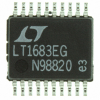
LT1738EG#TR Linear Technology, LT1738EG#TR Datasheet - Page 9

LT1738EG#TR
Manufacturer Part Number
LT1738EG#TR
Description
IC DC/DC CONTRLR LOW NOIS 20SSOP
Manufacturer
Linear Technology
Type
Step-Up (Boost), Cuk, Flybackr
Datasheet
1.LT1738EGPBF.pdf
(20 pages)
Specifications of LT1738EG#TR
Internal Switch(s)
No
Synchronous Rectifier
No
Number Of Outputs
1
Voltage - Output
5 ~ 100 V
Frequency - Switching
20kHz ~ 250kHz
Voltage - Input
2.55 ~ 20 V
Operating Temperature
-40°C ~ 125°C
Mounting Type
Surface Mount
Package / Case
20-SSOP
Lead Free Status / RoHS Status
Contains lead / RoHS non-compliant
Current - Output
-
Power - Output
-
Other names
LT1738EGTR
Available stocks
Company
Part Number
Manufacturer
Quantity
Price
OPERATIO
In noise sensitive applications switching regulators tend
to be ruled out as a power supply option due to their
propensity for generating unwanted noise. When switch-
ing supplies are required due to efficiency or input/output
constraints, great pains must be taken to work around the
noise generated by a typical supply. These steps may
include pre and post regulator filtering, precise synchro-
nization of the power supply oscillator to an external clock,
synchronizing the rest of the circuit to the power supply
oscillator or halting power supply switching during noise
sensitive operations. The LT1738 greatly simplifies the
task of eliminating supply noise by enabling the design of
an inherently low noise switching regulator power supply.
The LT1738 is a fixed frequency, current mode switching
regulator with unique circuitry to control the voltage and
current slew rates of the output switch. Current mode
control provides excellent AC and DC line regulation and
simplifies loop compensation.
Slew control capability provides much greater control
over the power supply components that can create con-
ducted and radiated electromagnetic interference. Com-
pliance with EMI standards will be an easier task and will
require fewer external filtering components.
The LT1738 uses an external N-channel MOSFET as the
power switch. This allows the user to tailor the drive
conditions to a wide range of voltages and currents.
CURRENT MODE CONTROL
Referring to the block diagram. A switching cycle begins
with an oscillator discharge pulse, which resets the RS
flip-flop, turning on the GATE driver and the external
MOSFET. The switch current is sensed across the external
sense resistor and the resulting voltage is amplified and
compared to the output of the error amplifier (V
driver is turned off once the output of the current sense
amplifier exceeds the voltage on the V
pulse by pulse current limit is achieved.
Internal slope compensation is provided to ensure stabil-
ity under high duty cycle conditions.
Output regulation is obtained using the error amp to set
the switch current trip point. The error amp is a
U
C
pin. In this way
C
pin). The
transconductance amplifier that integrates the difference
between the feedback output voltage and an internal
1.25V reference. The output of the error amp adjusts the
switch current trip point to provide the required load
current at the desired regulated output voltage. This
method of controlling current rather than voltage pro-
vides faster input transient response, cycle-by-cycle
current limiting for better output switch protection and
greater ease in compensating the feedback loop. The V
pin is used for loop compensation and current limit
adjustment. During normal operation the V
be between 0.25V and 1.27V. An external clamp on V
SS may be used for lowering the current limit.
The negative voltage feedback amplifier allows for direct
regulation of negative output voltages. The voltage on the
NFB pin gets amplified by a gain of – 0.5 and driven on to
the FB input, i.e., the NFB pin regulates to –2.5V while the
amplifier output internally drives the FB pin to 1.25V as in
normal operation. The negative feedback amplifier input
impedance is 100k (typ) referred to ground.
Soft-Start
Control of the switch current during start up can be
obtained by using the SS pin. An external capacitor from
SS to ground is charged by an internal 9 A current source.
The voltage on V
as the SS pin ramps up the V
ramp up. This will then provide for a smooth increase in
switch maximum current. SS will be discharged as a result
of the CS voltage exceeding the short circuit threshold of
approximately 0.22V.
Slew Control
Control of output voltage and current slew rates is achieved
via two feedback loops. One loop controls the MOSFET
drain dV/dt and the other loop controls the MOSFET dI/dt.
The voltage slew rate uses an external capacitor between
CAP and the MOSFET drain. This integrating cap closes the
voltage feedback loop. The external resistor R
current for the integrator. The voltage slew rate is thus
inversely proportional to both the value of capacitor and
R
VSL
.
C
cannot exceed the voltage on SS. Thus
C
voltage will be allowed to
C
LT1738
VSL
voltage will
sets the
1738fa
C
9
or
C


