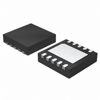
LTC3407EDD-3#TRPBF Linear Technology, LTC3407EDD-3#TRPBF Datasheet - Page 12

LTC3407EDD-3#TRPBF
Manufacturer Part Number
LTC3407EDD-3#TRPBF
Description
IC REG DC/DC DUAL STEPDOWN 10DFN
Manufacturer
Linear Technology
Type
Step-Down (Buck)r
Datasheet
1.LTC3407EDD-3PBF.pdf
(16 pages)
Specifications of LTC3407EDD-3#TRPBF
Internal Switch(s)
Yes
Synchronous Rectifier
Yes
Number Of Outputs
2
Voltage - Output
0.6 ~ 5 V
Current - Output
1A
Frequency - Switching
1.5MHz
Voltage - Input
2.5 ~ 5.5 V
Operating Temperature
-40°C ~ 85°C
Mounting Type
Surface Mount
Package / Case
10-DFN
Lead Free Status / RoHS Status
Lead free / RoHS Compliant
Power - Output
-
Available stocks
Company
Part Number
Manufacturer
Quantity
Price
APPLICATIONS INFORMATION
LTC3407-3
with a load current of 800mA and an ambient temperature
of 70°C. From the Typical Performance Characteristics
graph of Switch Resistance, the R
the main switch is 0.425Ω. Therefore, power dissipated
by each channel is:
The DFN package junction-to-ambient thermal resistance,
θ
the regulator operating in a 70°C ambient temperature is
approximately:
which is below the absolute maximum junction tempera-
ture of 125°C.
Design Example
As a design example, consider using the LTC3407-3 in
an portable application with a Li-Ion battery. The battery
provides a V
of 800mA in active mode and 2mA in standby mode. The
output voltage is V
power in standby, Burst Mode operation is selected for
good low load effi ciency.
First, calculate the inductor value for about 30% ripple
current at maximum V
12
JA
P
T
L
, is 40°C/W. Therefore, the junction temperature of
J
D
= 2 • 0.272 • 40 + 70 = 91.8°C
= I
2.25MHz • 300mA
OUT
IN
2
1.8V
• R
= 2.8V to 4.2V. The load requires a maximum
DS(ON)
OUT
IN
= 1.8V. Since the load still needs
= 272mW
:
• 1–
Figure 3. LTC3407-3 Layout Diagram (See Board Layout Checklist)
V
C
1.8V
4.2V
OUT2
OUT2
V
DS(ON)
IN
=1.5μH
BOLD LINES INDICATE
HIGH CURRENT PATH
resistance of
C
IN
L2
MODE/SYNC
SW2
V
RUN2
FB2
LTC3407-3
GND
V
IN
Choosing a vendor’s closest inductor value of 2.2μH,
results in a maximum ripple current of:
For cost reasons, a ceramic capacitor will be used. C
selection is then based on load step droop instead of ESR
requirements. For a 5% output droop:
A good standard value is 10μF . Since the output impedance
of a Li-Ion battery is very low, C
The POR pin is a common drain output and requires a pull-
up resistor. A 100k resistor is used for adequate speed.
Figure 1 shows the complete schematic for this design
example.
Board Layout Considerations
When laying out the printed circuit board, the following
checklist should be used to ensure proper operation of
the LTC3407-3. These items are also illustrated graphically
in the layout diagram of Figure 3. Check the following in
your layout:
1. Does the capacitor C
3) and GND (exposed pad) as close as possible? This
capacitor provides the AC current to the internal power
MOSFETs and their drivers.
C
RUN1
SW1
OUT
POR
V
I
L
FB1
=
≈ 2.5
2.25MHz • 2.2μH
L1
2.25MHz • (5% • 1.8V)
34073 F03
1.8V
C
V
OUT1
OUT1
800mA
IN
connect to the power V
• 1
IN
1.8V
4.2V
is typically 10μF .
= 9.9μF
= 208mA
IN
34073fb
(Pin
OUT


