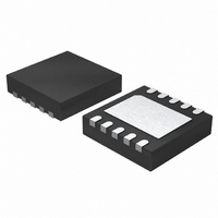
LTC3407EDD-3#TRPBF Linear Technology, LTC3407EDD-3#TRPBF Datasheet

LTC3407EDD-3#TRPBF
Specifications of LTC3407EDD-3#TRPBF
Available stocks
Related parts for LTC3407EDD-3#TRPBF
LTC3407EDD-3#TRPBF Summary of contents
Page 1
... In shutdown, the device draws <1μA. L, LT, LTC, LTM, Burst Mode, Linear Technology and the Linear logo are registered trademarks of Linear Technology Corporation. All other trademarks are the property of their respective owners. Protected by U.S. Patents, including 5481178, 6580258, 6304066, 6127815, 6498466, 6611131 ...
Page 2
... ORDERING INFORMATION LEAD FREE FINISH TAPE AND REEL LTC3407EDD-3#PBF LTC3407EDD-3#TRPBF Consult LTC Marketing for parts specifi ed with wider operating temperature ranges. Consult LTC Marketing for information on non-standard lead based fi nish parts. For more information on lead free part marking, go to: For more information on tape and reel specifi ...
Page 3
ELECTRICAL CHARACTERISTICS temperature range, otherwise specifi cations are at T SYMBOL PARAMETER I Peak Switch Current Limit, Channel 1 + LIM Channel 2 R Top Switch On-Resistance DS(ON) Bottom Switch On-Resistance I Switch Leakage Current SW(LKG) POR Power-On Reset Threshold ...
Page 4
LTC3407-3 TYPICAL PERFORMANCE CHARACTERISTICS Load Step V OUT 200mV/DIV I L 500mA/DIV I LOAD 500mA/DIV 34073 G04 20μs/DIV 3.3V OUT I = 80mA TO 800mA LOAD CIRCUIT OF FIGURE 1 Reference Voltage vs Temperature ...
Page 5
TYPICAL PERFORMANCE CHARACTERISTICS Load Regulation Burst Mode OPERATION 1 0 PULSE-SKIPPING –1 MODE –2 – 3.6V 1.8V IN OUT NO LOAD ON OTHER CHANNEL – 100 LOAD CURRENT (mA) 34073 G12 ...
Page 6
LTC3407-3 BLOCK DIAGRAM REGULATOR 1 6 MODE/SYNC + 0. OUT1 – R3 – 0.55V UVDET + + OVDET – 0.65V SHUTDOWN RUN1 2 0.6V REF OSC 9 RUN2 REGULATOR 2 (IDENTICAL TO REGULATOR 1) ...
Page 7
OPERATION The LTC3407-3 uses a constant frequency, current mode architecture. The operating frequency is set at 2.25MHz and can be synchronized to an external oscillator. Both channels share the same clock and run in-phase. To suit a variety of applications, ...
Page 8
LTC3407-3 APPLICATIONS INFORMATION A general LTC3407-3 application circuit is shown in Figure 2. External component selection is driven by the load requirement, and begins with the selection of the inductor L. Once the inductor is chosen, C can be selected. ...
Page 9
APPLICATIONS INFORMATION Output Capacitor (C ) Selection OUT The selection driven by the required ESR to OUT minimize voltage ripple and load step transients. Typically, once the ESR requirement is satisfi ed, the capacitance is adequate for ...
Page 10
... The solution is to limit the turn-on speed of the load switch driver. A Hot Swap™ controller is designed specifi cally for this purpose and usually incorporates cur- rent limiting, short-circuit protection, and soft-starting. Hot Swap is a trademark of Linear Technology Corporation. immediately shifts by an amount also begins to charge or dis- LOAD to its steady-state value ...
Page 11
APPLICATIONS INFORMATION Effi ciency Considerations The percent effi ciency of a switching regulator is equal to the output power divided by the input power times 100 often useful to analyze individual losses to determine what is limiting the ...
Page 12
LTC3407-3 APPLICATIONS INFORMATION with a load current of 800mA and an ambient temperature of 70°C. From the Typical Performance Characteristics graph of Switch Resistance, the R the main switch is 0.425Ω. Therefore, power dissipated by each channel is ...
Page 13
APPLICATIONS INFORMATION 2. Are the C and L1 closely connected? The (–) plate of OUT C returns current to GND and the (–) plate of C OUT 3. The output feedback line should be routed away from noisy components and ...
Page 14
LTC3407-3 TYPICAL APPLICATIONS OUT2 3.3V 800mA 10μF 14 1mm Height Core Supply C1* 10μF RUN2 V RUN1 IN POR MODE/SYNC L2 LTC3407-3 2.2μH 2.2μH SW2 SW1 OUT1 OUT2 GND C1, C2, C3: TAIYO ...
Page 15
... NOTE 6) 0.200 REF Information furnished by Linear Technology Corporation is believed to be accurate and reliable. However, no responsibility is assumed for its use. Linear Technology Corporation makes no representa- tion that the interconnection of its circuits as described herein will not infringe on existing patent rights. DD Package 10-Lead Plastic DFN (3mm × 3mm) (Reference LTC DWG # 05-08-1699 Rev B) 0 ...
Page 16
... Synchronous Step Down DC/DC Converter LTC3440 600mA (I ), 2MHz, OUT Synchronous Buck-Boost DC/DC Converter LTC3548/LTC3548-1 2.25MHz/400mA/800mA (I LTC3548-2 Synchronous Step-Down DC/DC Converter ThinSOT is a trademark of Linear Technology Corporation. Linear Technology Corporation 16 1630 McCarthy Blvd., Milpitas, CA 95035-7417 (408) 432-1900 FAX: (408) 434-0507 ● 2.8V TO 4.2V C1 10μ ...


