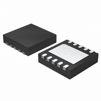
LTC3407EDD-4#PBF Linear Technology, LTC3407EDD-4#PBF Datasheet - Page 5

LTC3407EDD-4#PBF
Manufacturer Part Number
LTC3407EDD-4#PBF
Description
IC REG DC/DC DUAL STEPDOWN 10DFN
Manufacturer
Linear Technology
Type
Step-Down (Buck)r
Datasheet
1.LTC3407EDD-4PBF.pdf
(16 pages)
Specifications of LTC3407EDD-4#PBF
Internal Switch(s)
Yes
Synchronous Rectifier
Yes
Number Of Outputs
2
Voltage - Output
0.6 ~ 5 V
Current - Output
1A
Frequency - Switching
1.5MHz
Voltage - Input
2.5 ~ 5.5 V
Operating Temperature
-40°C ~ 85°C
Mounting Type
Surface Mount
Package / Case
10-DFN
Lead Free Status / RoHS Status
Lead free / RoHS Compliant
Power - Output
-
Available stocks
Company
Part Number
Manufacturer
Quantity
Price
TYPICAL PERFORMANCE CHARACTERISTICS
PIN FUNCTIONS
V
age from the external resistive divider across the output.
Nominal voltage for this pin is 0.6V.
RUN1 (Pin 2): Regulator 1 Enable. Forcing this pin to V
enables regulator 1, while forcing it to GND causes regulator
1 to shut down. This pin must be driven; do not fl oat.
V
to GND.
SW1 (Pin 4): Regulator 1 Switch Node Connection to the
Inductor. This pin swings from V
GND (Pin 5): Ground. This pin is not connected internally.
Connect to PCB ground for shielding.
MODE/SYNC (Pin 6): Combination Mode Selection and
Oscillator Synchronization. This pin controls the opera-
tion of the device. When tied to V
operation or pulse-skipping mode is selected, respectively.
Do not fl oat this pin. The oscillation frequency can be
FB1
IN
100
(Pin 3): Main Power Supply. Must be closely decoupled
90
80
70
60
50
40
30
20
10
0
(Pin 1): Output Feedback. Receives the feedback volt-
1
Effi ciency vs Load Current
V
Burst Mode OPERATION
NO LOAD ON OTHER CHANNEL
OUT
= 1.2V
V
IN
= 3.6V
LOAD CURRENT (mA)
10
V
IN
= 4.2V
V
IN
100
= 2.7V
34074 G13
IN
IN
1000
to GND.
or GND, Burst Mode
100
90
80
70
60
Effi ciency vs Load Current
1
V
Burst Mode OPERATION
NO LOAD ON OTHER CHANNEL
OUT
= 1.5V
V
IN
= 3.6V
LOAD CURRENT (mA)
IN
10
V
IN
synchronized to an external oscillator applied to this pin
and pulse-skipping mode is automatically selected.
SW2 (Pin 7): Regulator 2 Switch Node Connection to the
Inductor. This pin swings from V
POR (Pin 8): Power-On Reset . This common-drain logic
output is pulled to GND when the output voltage is not
within ±8.5% of regulation and goes high after 29ms when
both channels are within regulation.
RUN2 (Pin 9): Regulator 2 Enable. Forcing this pin to V
enables regulator 2, while forcing it to GND causes regulator
2 to shut down. This pin must be driven; do not fl oat.
V
voltage from the external resistive divider across the output.
Nominal voltage for this pin is 0.6V.
Exposed Pad (GND) (Pin 11): Power Ground. Connect to
the (–) terminal of C
connected to electrical ground on PCB.
= 4.2V
FB2
V
100
IN
(Pin 10): Output Feedback. Receives the feedback
= 2.7V
34074 G14
1000
OUT
–0.2
–0.4
–0.6
–0.8
–1.0
0.8
0.6
0.4
0.2
, and (–) terminal of C
0
2
Line Regulation
V
I
T
OUT
A
OUT
= 25°C
= 200mA
= 1.8V
3
IN
to GND.
LTC3407-4
V
IN
4
(V)
IN
. Must be
5
34074 G15
34074fa
5
IN
6


