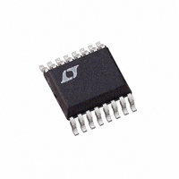
LTC1735CGN-1 Linear Technology, LTC1735CGN-1 Datasheet - Page 25

LTC1735CGN-1
Manufacturer Part Number
LTC1735CGN-1
Description
IC SW REG STEP-DOWN SYNC 16-SSOP
Manufacturer
Linear Technology
Type
Step-Down (Buck)r
Datasheet
1.LTC1735CGN-1PBF.pdf
(28 pages)
Specifications of LTC1735CGN-1
Internal Switch(s)
No
Synchronous Rectifier
Yes
Number Of Outputs
1
Voltage - Output
0.8 ~ 6 V
Current - Output
3A
Frequency - Switching
300kHz
Voltage - Input
4 ~ 30 V
Operating Temperature
0°C ~ 85°C
Mounting Type
Surface Mount
Package / Case
16-SSOP
Lead Free Status / RoHS Status
Contains lead / RoHS non-compliant
Power - Output
-
Available stocks
Company
Part Number
Manufacturer
Quantity
Price
Company:
Part Number:
LTC1735CGN-1
Manufacturer:
Linear Technology
Quantity:
135
Part Number:
LTC1735CGN-1
Manufacturer:
LINEAR
Quantity:
20 000
Part Number:
LTC1735CGN-1#PBF
Manufacturer:
LT/凌特
Quantity:
20 000
Part Number:
LTC1735CGN-1#TRPBF
Manufacturer:
LINEAR/凌特
Quantity:
20 000
APPLICATIO S I FOR ATIO
3. Are the SENSE
4. Does the (+) terminal of C
LTC1735-1. The V
close to any other nodes with high slew rates.
minimum PC trace spacing? The filter capacitor be-
tween SENSE
possible to the LTC1735-1. Ensure accurate current
sensing with kelvin connections to the SENSE resistors
shown in Figure 13. Series resistance can be added to
the SENSE lines to increase noise rejection.
topside MOSFET(s) as closely as possible? This capaci-
tor provides the AC current to the MOSFET(s).
+
+
and SENSE
and SENSE
U
C
C
SS
C2
R
OSENSE
C
U
C
C
IN
OSC
C
1000pF
47pF
line should not be routed
–
connect to the drain of the
INTV
leads routed together with
–
should be as close as
CC
1
2
3
4
5
6
7
8
W
C
RUN/SS
I
PGOOD
SENSE
SENSE
V
SGND
TH
OSC
OSENSE
LTC1735-1
–
+
Figure 12. LTC1735-1 Layout Diagram
Figure 13. Kelvin Sensing R
EXTV
U
INTV
BOOST
PGND
SW
V
BG
TG
CC
CC
IN
HIGH CURRENT PATH
SENSE
16
15
14
13
12
11
10
9
R1
R2
+
+
SENSE
+
5. Is the INTV
6. Keep the switching node (SW), Top Gate node (TG), and
C
4.7 F
OUT
D
–
between INTV
tor carries the MOSFET driver peak currents. An addi-
tional 1 F ceramic placed immediately next to the INTV
and PGND pins can help improve noise performance.
Boost node (BOOST) away from sensitive small-signal
nodes, especially from the voltage and current sensing
feedback pins. All of these nodes have very large and
fast moving signals and therefore should be kept on the
“output side” (Pins 9 to 16) of the LTC1735-1 and
occupy minimum PC trace area.
B
SENSE
C
B
CURRENT SENSE
RESISTOR
(R
SENSE
CC
Q1
R
L1
1735-1 F13
SENSE
CC
)
decoupling capacitor connected closely
and the power ground pin? This capaci-
D1
Q2
C
IN
1735-1 F12
LTC1735-1
V
V
OUT
+
–
–
+
IN
25
CC


