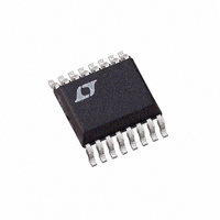
LTC1735CGN-1 Linear Technology, LTC1735CGN-1 Datasheet - Page 16

LTC1735CGN-1
Manufacturer Part Number
LTC1735CGN-1
Description
IC SW REG STEP-DOWN SYNC 16-SSOP
Manufacturer
Linear Technology
Type
Step-Down (Buck)r
Datasheet
1.LTC1735CGN-1PBF.pdf
(28 pages)
Specifications of LTC1735CGN-1
Internal Switch(s)
No
Synchronous Rectifier
Yes
Number Of Outputs
1
Voltage - Output
0.8 ~ 6 V
Current - Output
3A
Frequency - Switching
300kHz
Voltage - Input
4 ~ 30 V
Operating Temperature
0°C ~ 85°C
Mounting Type
Surface Mount
Package / Case
16-SSOP
Lead Free Status / RoHS Status
Contains lead / RoHS non-compliant
Power - Output
-
Available stocks
Company
Part Number
Manufacturer
Quantity
Price
Company:
Part Number:
LTC1735CGN-1
Manufacturer:
Linear Technology
Quantity:
135
Part Number:
LTC1735CGN-1
Manufacturer:
LINEAR
Quantity:
20 000
Part Number:
LTC1735CGN-1#PBF
Manufacturer:
LT/凌特
Quantity:
20 000
Part Number:
LTC1735CGN-1#TRPBF
Manufacturer:
LINEAR/凌特
Quantity:
20 000
When adjusting the gate drive level, the final arbiter is the
total input current for the regulator. If you make a change
and the input current decreases, then you improved the
efficiency. If there is no change in input current, then there
is no change in efficiency.
SENSE
The common mode input range of the current comparator
is from 0V to 1.1(INTV
guaranteed throughout this range allowing output volt-
ages anywhere from 0.8V to 7V. A differential NPN input
stage is used and is biased with internal resistors from an
internal 2.4V source as shown in the Functional Diagram.
This causes current either to be sourced or sunk by these
pins depending on the output voltage. If the output voltage
is below 2.4V, current will flow out of both SENSE pins to
the main output. This forces a minimum load current that
can be fulfilled by the V
mum current flowing out of the SENSE pins is:
Since V
can choose R1 in Figure 3 to have a maximum value to
absorb this current:
Regulating an output voltage of 1.8V, the maximum value
of R1 should be 32k. Note that for output voltages above
2.4V no maximum value of R1 is necessary to absorb the
sense currents; however, R1 is still bounded by the
V
Soft-Start/Run Function
The RUN/SS pin is a multipurpose pin that provides a soft-
start function and a means to shut down the LTC1735-1.
Soft-start reduces surge currents from V
increasing the controller’s current limit I
can also be used for power supply sequencing.
Pulling the RUN/SS pin below 1.5V puts the LTC1735-1
into a low quiescent current shutdown (I
pin can be driven directly from logic as shown in Figures
4 and 5. Releasing the RUN/SS pin allows an internal
1.2 A current source to charge up the external soft-start
LTC1735-1
APPLICATIO S I FOR ATIO
16
OSENSE
I
SENSE
R Max
1
(
+
OSENSE
/ SENSE
+
feedback current.
+ I
)
SENSE
24
is servoed to the 0.8V reference voltage, we
–
k
–
Pins
= (2.4V – V
U
2 4
.
CC
V V
0 8
OUT
). Continuous linear operation is
.
–
U
V
OUT
resistive divider. The maxi-
OUT
)/24k
W
TH(MAX)
Q
IN
< 25 A). This
by gradually
U
. This pin
capacitor C
ground there is a delay before starting of approximately:
When the voltage on RUN/SS reaches 1.5V the
LTC1735-1 begins operating with a current limit at ap-
proximately 25mV/R
increases from 1.5V to 3V, the internal current limit is
increased from 25mV/R
put current limit ramps up slowly, taking an additional
1.25s/ F to reach full current. Ramping the output cur-
rent slowly reduces the starting surge current
required from the input supply.
Diode D1 in Figure 4 and Figure 5 reduces the start delay
while allowing C
function. This diode and C
not needed. The RUN/SS pin has an internal 6V zener
clamp (see Functional Diagram).
Fault Conditions: Overcurrent Latchoff
The RUN/SS pin also provides the ability to shut off the
controller and latchoff when an overcurrent condition is
detected. The RUN/SS capacitor C
turn on and limit the inrush current of the controller. After
the controller has been started and given adequate time to
charge up the output capacitor and provide full load
3.3V OR 5V
T
Figure 5. RUN/SS Pin Interfacing with Latchoff Defeated
DELAY
3.3V OR 5V
SS.
D1
1 2
1 5
(a)
Figure 4. RUN/SS Pin Interfacing
.
If RUN/SS has been pulled all the way to
D1
.
V
IN
SS
V
R
A
SS
to charge up slowly for the soft-start
RUN/SS
C
RUN/SS
SS
SENSE
SENSE
C
SS
C
SS
SS
. As the voltage on RUN/SS
1 25
can be deleted if soft-start is
.
to 75mV/R
s F C
/
SS
INTV
is used initially to
SS
CC
R
D1
SENSE
SS
(b)
RUN/SS
RUN/SS
. The out-
1735-1 F04
1735-1 F05
C
C
SS
SS


