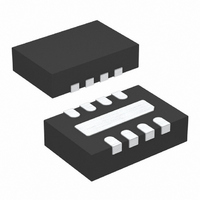
LTC3531EDD-3.3#TRPBF Linear Technology, LTC3531EDD-3.3#TRPBF Datasheet - Page 9

LTC3531EDD-3.3#TRPBF
Manufacturer Part Number
LTC3531EDD-3.3#TRPBF
Description
IC DC/DC CONV 200MA 8-DFN
Manufacturer
Linear Technology
Type
Step-Down (Buck), Step-Up (Boost)r
Datasheet
1.LTC3531EDDPBF.pdf
(16 pages)
Specifications of LTC3531EDD-3.3#TRPBF
Internal Switch(s)
Yes
Synchronous Rectifier
Yes
Number Of Outputs
1
Voltage - Output
3.3V
Current - Output
200mA
Voltage - Input
1.8 ~ 5.5 V
Operating Temperature
-40°C ~ 85°C
Mounting Type
Surface Mount
Package / Case
8-DFN
Lead Free Status / RoHS Status
Lead free / RoHS Compliant
Power - Output
-
Frequency - Switching
-
Available stocks
Company
Part Number
Manufacturer
Quantity
Price
OPERATIO
The LTC3531, LTC3531-3.3 and LTC3531-3 synchro-
nous buck-boost converters utilize a Burst Mode control
technique to achieve high effi ciency over a wide dynamic
range of load currents. A 2% accurate comparator is
used to monitor the output voltage. If V
programmed reference threshold no switching occurs and
only quiescent current is drawn from the power source
(sleep mode). When V
threshold the IC “wakes up”, switching commences, and
the output capacitor is charged. The value of the output
capacitor, the load current, and the comparator hysteresis
(~1%) determines the number of current pulses required
to pump-up the output capacitor before the part returns
to sleep.
In order to determine the best operating mode for the
converter, the LTC3531 contains a second comparator
that monitors the relative voltage difference between V
and V
as well as typical inductor currents are shown in Figure 1.
Regions of the current waveforms where switches A and
D are on provide the highest effi ciency since energy is
transferred directly from the input source to the output.
Boost Mode
If V
boost or step-up mode. Referring to Figure 1 (left side)
when V
and C are turned on (V
and current is ramped until I
IN
OUT
is ~400mV below V
OUT
. Input and output voltages in the various modes
falls below its regulation voltage, switches A
V
IN
SW1
A
B
U
L
IN
OUT
is applied across the inductor)
OUT
D
SW2
C
drops below the reference
PEAK
, the LTC3531 operates in
V
OUT
is detected. When this
I
VALLEY
I
I
V
I
ZERO
PEAK
MAX
OUT
Figure 1. Voltage and Current Waveforms
OUT
V
IN
AC
is above its
BOOST MODE
AD
AC
AD
IN
AC
occurs, C is turned off, D is turned on and current is deliv-
ered to the output capacitor (V
the inductor). Inductor current falls when D is on, until an
I
results in an increased load current capability for a given
peak current. This AC then AD switch sequence is repeated
until the output is pumped above its regulation voltage, a
fi nal I
(I
V
4-Switch Mode
If (V
operates in 4-switch step-up/down mode. Returning to
Figure 1 (center) when V
age, switches A and C are turned on and current is ramped
until I
is then turned off, D is turned on and current is delivered
to the output. When A and D are on, the inductor current
slope is dependant on the relationship between V
and the R
timer (approximately 3μs) is used to terminate the AD
pulse. Once the t
B is turned on and inductor current is ramped down (V
is applied across the inductor) until I
This sequence is repeated until the output is regulated,
BD switches are turned on, and a fi nal I
Anticross conduction circuitry in all modes ensures the
P-channel MOSFET and N-channel MOSFET switch pairs (A
and B or D and C) are never turned on simultaneously.
t
VALLEY
OFF
OUT
VALLEY
AD
OUT
BD
ZERO
is above its programmed value).
PEAK
AC
4SW MODE
is detected. Terminating at I
– 400mV) < ~V
LTC3531-3.3/LTC3531-3
is ignored and I
t
AD
DSON
OFF
is detected, and the part returns to sleep mode
is detected. As with Boost Mode operation, C
BD
AC
of the switches. In 4-switch mode, a t
OFF
t
OFF
AD
timer expires, switch A is turned off,
BD
IN
OUT
ZERO
< (V
falls below its regulation volt-
OUT
AD
IN
is used in all modes once
BUCK MODE
– V
VALLEY
+ 800mV), the LTC3531
BD
OUT
AD
LTC3531/
VALLEY
BD
, rather than I
is applied across
ZERO
V
IN
3531 F01
is detected.
is detected.
IN
, V
ZERO
3531fb
OUT
9
OUT
OFF
,
,


