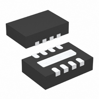
LTC3531EDD-3.3#TRPBF Linear Technology, LTC3531EDD-3.3#TRPBF Datasheet - Page 7

LTC3531EDD-3.3#TRPBF
Manufacturer Part Number
LTC3531EDD-3.3#TRPBF
Description
IC DC/DC CONV 200MA 8-DFN
Manufacturer
Linear Technology
Type
Step-Down (Buck), Step-Up (Boost)r
Datasheet
1.LTC3531EDDPBF.pdf
(16 pages)
Specifications of LTC3531EDD-3.3#TRPBF
Internal Switch(s)
Yes
Synchronous Rectifier
Yes
Number Of Outputs
1
Voltage - Output
3.3V
Current - Output
200mA
Voltage - Input
1.8 ~ 5.5 V
Operating Temperature
-40°C ~ 85°C
Mounting Type
Surface Mount
Package / Case
8-DFN
Lead Free Status / RoHS Status
Lead free / RoHS Compliant
Power - Output
-
Frequency - Switching
-
Available stocks
Company
Part Number
Manufacturer
Quantity
Price
PI FU CTIO S
SW2 (Pin 1/Pin 7): Buck-Boost Switch Pin Where Internal
Switches C and D are Connected. An optional Schottky
diode can be connected from SW2 to V
effi ciency improvement. Minimize trace length to keep
EMI down.
GND (Pin 2/Pin 3): Signal Ground for the IC.
PGND (Pin 2/Pin 8): Power Ground for the IC. (Shared
on ThinSOT version)
V
Rectifi er. A fi lter capacitor is placed from V
A ceramic bypass capacitor is recommended as close to
the V
SHDN (Pin 4/Pin 4): External Shutdown Pin. An applied
voltage of < 0.4V shuts down the converter. A voltage
above >1.4V will enable the converter.
OUT
U
(Pin 3/Pin 6): Output of the Buck-Boost Synchronous
OUT
and GND pins as possible.
U
U
ThinSOT/DFN Packages
OUT
for a moderate
OUT
to GND.
V
Converter. A minimum 2.2μF Ceramic Capacitor should
be placed between V
FB (NA/Pin 5): Feedback Pin for the Adjustable Version.
Connect the resistor divider tap here. The output voltage
can be adjusted from 2V to 5V.
SW1 (Pin 6/Pin 1): Buck-Boost Switch Pin Where Internal
Switches A and B are Connected. Connect the inductor
from SW1 to SW2.
Exposed Pad (Pin 9, DFN): Solder to PCB ground for
optimal thermal performance.
IN
V
(Pin 5/Pin 2): Input Supply Pin for the Buck-Boost
OUT
LTC3531-3.3/LTC3531-3
=
1 225 1
.
⎛
⎝ ⎜
+
IN
R
R
and GND.
2
1
⎞
⎠ ⎟
LTC3531/
3531fb
7


