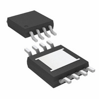
LTC3448EMS8E Linear Technology, LTC3448EMS8E Datasheet - Page 13

LTC3448EMS8E
Manufacturer Part Number
LTC3448EMS8E
Description
IC CONV DC/DC SYNC STEPDWN 8MSOP
Manufacturer
Linear Technology
Type
Step-Down (Buck)r
Datasheet
1.LTC3448EDD.pdf
(20 pages)
Specifications of LTC3448EMS8E
Internal Switch(s)
Yes
Synchronous Rectifier
Yes
Number Of Outputs
1
Voltage - Output
0.6 ~ 5.2 V
Current - Output
600mA
Frequency - Switching
1.5MHz ~ 2.25MHz
Voltage - Input
2.5 ~ 5.5 V
Operating Temperature
-40°C ~ 85°C
Mounting Type
Surface Mount
Package / Case
8-MSOP Exposed Pad, 8-HMSOP, 8-eMSOP
Lead Free Status / RoHS Status
Contains lead / RoHS non-compliant
Power - Output
-
Available stocks
Company
Part Number
Manufacturer
Quantity
Price
Company:
Part Number:
LTC3448EMS8E
Manufacturer:
LT
Quantity:
10 000
Part Number:
LTC3448EMS8E#PBF
Manufacturer:
LINEAR/凌特
Quantity:
20 000
Company:
Part Number:
LTC3448EMS8E-1.5
Manufacturer:
LT
Quantity:
10 000
Company:
Part Number:
LTC3448EMS8E-1.8
Manufacturer:
LT
Quantity:
10 000
APPLICATIO S I FOR ATIO
with C
deliver enough current to prevent this problem if the load
switch resistance is low and it is driven quickly. The only
solution is to limit the rise time of the switch drive so that
the load rise time is limited to approximately (25 • C
Thus, a 10µF capacitor charging to 3.3V would require a
250µs rise time, limiting the charging current to about
130mA.
PC Board Layout Checklist
When laying out the printed circuit board, the following
checklist should be used to ensure proper operation of the
LTC3448. These items are also illustrated graphically in
Figures 7 and 8. Check the following in your layout:
1. The power traces, consisting of the GND trace, the SW
trace and the V
wide.
OUT
, causing a rapid drop in V
IN
U
trace should be kept short, direct and
U
V
IN
W
OUT
. No regulator can
C
IN
4
8
6
7
Figure 7. LTC3448 Layout Design
V
RUN
FREQ
SYNC
U
IN
LTC3448
Figure 8. LTC3448 Layout
GND
MODE
LOAD
9
V
SW
OUT
V
FB
5
2
1
).
3
L
2. Does the V
3. Does the (+) plate of C
4. Keep the switching node, SW, away from the sensitive
5. Keep the (–) plates of C
Design Example
As a design example, assume the LTC3448 is used in a
single lithium-ion battery-powered cellular phone
application. The V
4.2V down to about 2.7V. The load current requirement
is a maximum of 0.6A but most of the time it will be in
standby mode, requiring only 2mA. Efficiency at both low
R
R
resistors? The resistive divider R1/R2 must be con-
nected between the (+) plate of C
possible? This capacitor provides the AC current to the
internal power MOSFETs.
V
FB2
FB1
FB
node.
3448 F07
C
FF
FB
3448 F08
IN
C
pin connect directly to the feedback
OUT
will be operating from a maximum of
V
OUT
IN
IN
and C
connect to V
OUT
OUT
as close as possible.
and ground.
IN
LTC3448
as closely as
13
3448f


