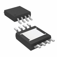
LTC3448EMS8E Linear Technology, LTC3448EMS8E Datasheet

LTC3448EMS8E
Specifications of LTC3448EMS8E
Available stocks
Related parts for LTC3448EMS8E
LTC3448EMS8E Summary of contents
Page 1
... Digital Still Cameras ■ MP3 Players ■ Portable Instruments , LTC and LT are registered trademarks of Linear Technology Corporation. All other trademarks are the property of their respective owners. Protected by U.S. Patents including 5481178, 6580258, 6304066, 6127815, 6498466, 6611131. Others pending. U TYPICAL APPLICATIO 1 ...
Page 2
... V ) • 100/V OVL OVL OUT OUT V = 2.5V to 5.5V (LDO 0. 90%, FB OUT Duty Cycle < 35% LDO, 1mA to 10mA (Note 9) ORDER PART NUMBER TOP VIEW LTC3448EMS8E 8 RUN 7 SYNC 9 6 FREQ 5 SW MS8 PART MARKING = 40° LTBMK MIN TYP MAX ±30 ● 0.5880 ...
Page 3
ELECTRICAL CHARACTERISTICS temperature range, otherwise specifications are T SYMBOL PARAMETER I Input DC Bias Current S Active Mode (Pulse Skip, No LRO) Linear Regulator Operation (LRO) Shutdown f Oscillator Frequency OSC f Synchronization Frequency SYNC V SYNC Activation Input Threshold ...
Page 4
LTC3448 W U TYPICAL PERFOR A CE CHARACTERISTICS (From Figure1a Except for the Resistive Divider Resistor Values) Efficiency vs Input Voltage 100 V = 1.8V OUT I = 100mA 95 OUT T = 25° 30mA 85 ...
Page 5
W U TYPICAL PERFOR A CE CHARACTERISTICS (From Figure1a Except for the Resistive Divider Resistor Values Temperature DS(ON) 0.6 0.5 0.4 0.3 0.2 MAIN SWITCH SYNCH SWITCH 2.5V 2.5V 0.1 3.6V 3.6V 4.2V 4.2V 0 – ...
Page 6
LTC3448 W U TYPICAL PERFOR A CE CHARACTERISTICS (From Figure 1a Except for the Resistive Divider Resistor Values) Load Step V OUT 100mV/DIV AC COUPLED I LOAD 250mA/DIV I L 500mA/DIV V = 3.6V 10µs/DIV 1.5V OUT ...
Page 7
CTIO AL DIAGRA SYNC 7 FREQ OSC V OUT LDO 2 DRIVE RUN 0.6V REF 8 0.6V + ∆OVL SHUTDOWN U OPERATIO (Refer to Functional Diagram) Main Control Loop ...
Page 8
LTC3448 U OPERATIO (Refer to Functional Diagram) the V pin and both the main and synchronous switches OUT are turned off. The control loop is stabilized by the load capacitor and requires a minimum value of 2µF. The LTC3448 will ...
Page 9
U OPERATIO (Refer to Functional Diagram) 1200 1000 V = 1.8V OUT 800 V = 2.5V OUT V = 1.5V OUT 600 400 200 0 2.5 3.5 4.0 4.5 3.0 SUPPLY VOLTAGE (V) Figure 4. Maximum Output Current vs Input ...
Page 10
LTC3448 U U APPLICATIO S I FOR ATIO Inductor Core Selection Different core materials and shapes will change the size/ current and price/current relationship of an inductor. Toroid or shielded pot cores in ferrite or permalloy mate- rials are small ...
Page 11
U U APPLICATIO S I FOR ATIO worst, a sudden inrush of current through the long wires can potentially cause a voltage spike damage the part. When choosing the input and output ceramic capacitors, choose the X5R ...
Page 12
LTC3448 U U APPLICATIO S I FOR ATIO top and bottom MOSFET R DS(ON) (DC) as follows )(DC DS(ON)TOP The R for both the top and bottom MOSFETs can DS(ON) be obtained from the ...
Page 13
U U APPLICATIO S I FOR ATIO with C , causing a rapid drop in V OUT deliver enough current to prevent this problem if the load switch resistance is low and it is driven quickly. The only solution is ...
Page 14
LTC3448 U U APPLICATIO S I FOR ATIO and high load currents is important. Output voltage is 1.8V. With this information we can calculate L using Equation (1), ⎛ ⎞ − OUT ( ) ( ) L ...
Page 15
U TYPICAL APPLICATIO S Single Li-Ion 1.5V/600mA Regulator for High Efficiency and Small Footprint 2.2µ RUN V OUT 4.7µF LTC3448 CER 3 MODE 6 1 FREQ ...
Page 16
LTC3448 U TYPICAL APPLICATIO S Single Li-Ion 1.2V/600mA Regulator for High Efficiency and Small Footprint 2.2µ RUN V OUT 4.7µF LTC3448 CER 3 MODE 6 1 ...
Page 17
U TYPICAL APPLICATIO S Single Li-Ion 2.5V/600mA Regulator with 1.8MHz External 2.5V TO 5.5V Load Step V OUT 100mV/DIV AC COUPLED LDOCNTRL 2V/DIV I LOAD 250mA/DIV V = 3.6V 40µs/DIV 2.5V OUT I = 100µA TO 300mA ...
Page 18
LTC3448 PACKAGE DESCRIPTIO 3.5 ±0.05 1.65 ±0.05 2.15 ±0.05 (2 SIDES) 0.25 ± 0.05 RECOMMENDED SOLDER PAD PITCH AND DIMENSIONS PIN 1 TOP MARK (NOTE 6) 0.200 REF Package 8-Lead Plastic DFN (3mm × 3mm) (Reference LTC ...
Page 19
... LEAD COPLANARITY (BOTTOM OF LEADS AFTER FORMING) SHALL BE 0.102mm (.004") MAX Information furnished by Linear Technology Corporation is believed to be accurate and reliable. However, no responsibility is assumed for its use. Linear Technology Corporation makes no represen- tation that the interconnection of its circuits as described herein will not infringe on existing patent rights. ...
Page 20
... IN OUT Q ≥ 2.5V 2.5V to 5.5V 25µA, IN OUT Q ≥ 2.4V to 5.25V 2.4V to 5.5V OUT ≥ 2.4V to 5.25V 2.4V to 5.5V OUT ≥ 2.4V to 5.25V 2.4V to 5.5V OUT LT/TP 0505 500 • PRINTED IN USA © LINEAR TECHNOLOGY CORPORATION 2005 = 25µ 35µ 28µA, Q 3448f ...


