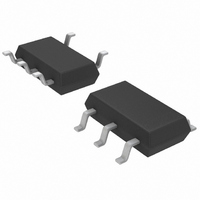
LTC3406BES5-1.2#TRM Linear Technology, LTC3406BES5-1.2#TRM Datasheet - Page 9

LTC3406BES5-1.2#TRM
Manufacturer Part Number
LTC3406BES5-1.2#TRM
Description
IC CNV 1.2V SYNC STPDWN TSOT23-5
Manufacturer
Linear Technology
Type
Step-Down (Buck)r
Datasheet
1.LTC3406BES5-1.2TRPBF.pdf
(12 pages)
Specifications of LTC3406BES5-1.2#TRM
Internal Switch(s)
Yes
Synchronous Rectifier
Yes
Number Of Outputs
1
Voltage - Output
1.2V
Current - Output
600mA
Frequency - Switching
1.5MHz
Voltage - Input
2.5 ~ 5.5 V
Operating Temperature
-40°C ~ 85°C
Mounting Type
Surface Mount
Package / Case
TSOT-23-5, TSOT-5, TSOP-5
Lead Free Status / RoHS Status
Contains lead / RoHS non-compliant
Power - Output
-
Other names
LTC3406BES5-1.2#TRMTR
Available stocks
Company
Part Number
Manufacturer
Quantity
Price
APPLICATIO S I FOR ATIO
1. The V
2. I
Other losses including C
losses and inductor core losses generally account for less
than 2% total additional loss.
Thermal Considerations
In most applications the LTC3406B-1.2 does not dissi-
pate much heat due to its high efficiency. But, in applica-
tions where the LTC3406B-1.2 is running at high ambient
temperature with low supply voltage, the heat dissipated
may exceed the maximum junction temperature of the
part. If the junction temperature reaches approximately
150°C, both power switches will be turned off and the SW
node will become high impedance.
the DC bias current as given in the electrical character-
istics and the internal main switch and synchronous
switch gate charge currents. The gate charge current
results from switching the gate capacitance of the
internal power MOSFET switches. Each time the gate is
switched from high to low to high again, a packet of
charge, dQ, moves from V
dQ/dt is the current out of V
the DC bias current. In continuous mode, I
f(Q
internal top and bottom switches. Both the DC bias and
gate charge losses are proportional to V
their effects will be more pronounced at higher supply
voltages.
internal switches, R
continuous mode, the average output current flowing
through inductor L is “chopped” between the main
switch and the synchronous switch. Thus, the series
resistance looking into the SW pin is a function of both
top and bottom MOSFET R
(DC) as follows:
The R
be obtained from the Typical Performance Charateristics
curves. Thus, to obtain I
R
output current.
2
L
R losses are calculated from the resistances of the
R
T
and multiply the result by the square of the average
SW
+ Q
IN
DS(ON)
= (R
B
quiescent current is due to two components:
) where Q
DS(ON)TOP
for both the top and bottom MOSFETs can
U
T
and Q
SW
)(DC) + (R
U
, and external inductor R
IN
2
R losses, simply add R
B
IN
and C
IN
are the gate charges of the
DS(ON)
that is typically larger than
to ground. The resulting
DS(ON)BOT
W
OUT
and the duty cycle
ESR dissipative
)(1 – DC)
IN
U
GATECHG
and thus
SW
L
. In
(2)
to
=
To avoid the LTC3406B-1.2 from exceeding the maximum
junction temperature, the user will need to do some
thermal analysis. The goal of the thermal analysis is to
determine whether the power dissipated exceeds the
maximum junction temperature of the part. The tempera-
ture rise is given by:
where P
is the thermal resistance from the junction of the die to the
ambient temperature.
The junction temperature, T
where T
As an example, consider the LTC3406B-1.2 with an input
voltage of 2.7V, a load current of 600mA and an ambient
temperature of 70°C. From the typical performance graph
of switch resistance, the R
0.52Ω for the P-channel switch and 0.42Ω for the
N-channel switch. Using equation (2) to find the series
resistance looking into the SW pin gives:
Therefore, power dissipated by the part is:
For the SOT-23 package, the θ
junction temperature of the regulator is:
which is below the maximum junction temperature of
125°C.
Note that at higher supply voltages, the junction tempera-
ture is lower due to reduced switch resistance (R
Checking Transient Response
The regulator loop response can be checked by looking at
the load transient response. Switching regulators take
several cycles to respond to a step in load current. When
a load step occurs, V
equal to (∆I
resistance of C
discharge C
T
T
R
P
T
R
J
J
D
SW
= T
= 70°C + (0.1656)(250) = 111.4°C
= (P
= I
= 0.52Ω(0.44) + 0.42Ω(0.56) = 0.46Ω
D
A
A
LOAD
is the power dissipated by the regulator and θ
is the ambient temperature.
D
+ T
)(θ
LOAD
OUT
2
R
JA
• R
, which generates a feedback error signal.
OUT
)
• ESR), where ESR is the effective series
SW
. ∆I
OUT
= 165.6mW
LOAD
immediately shifts by an amount
DS(ON)
J
, is given by:
also begins to charge or
JA
at 70°C is approximately
LTC3406B-1.2
is 250°C/ W. Thus, the
sn3406b12 3406b12fs
SW
).
9
JA


