LTC3406BES5-1.2#TRMPBF Linear Technology, LTC3406BES5-1.2#TRMPBF Datasheet
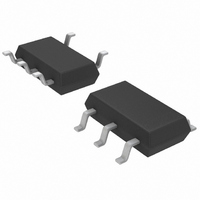
IC CNV 1.2V SYNC STPDWN TSOT23-5

LTC3406BES5-1.2#TRMPBF

Manufacturer Part Number
LTC3406BES5-1.2#TRMPBF
Description
IC CNV 1.2V SYNC STPDWN TSOT23-5
Manufacturer
Linear Technology
Type
Step-Down (Buck)r
Datasheet

Specifications of LTC3406BES5-1.2#TRMPBF

Internal Switch(s)
Yes
Synchronous Rectifier
Yes
Number Of Outputs
1
Voltage - Output
1.2V
Current - Output
600mA
Frequency - Switching
1.5MHz
Voltage - Input
2.5 ~ 5.5 V
Operating Temperature
-40°C ~ 85°C
Mounting Type
Surface Mount
Package / Case
TSOT-23-5, TSOT-5, TSOP-5
Dc To Dc Converter Type
Step Down
Pin Count
5
Input Voltage
5.5V
Output Voltage
1.2V
Switching Freq
210kHz
Output Current
600mA
Efficiency
96%
Package Type
TSOT-23
Output Type
Fixed
Switching Regulator
Yes
Load Regulation
0.5%
Line Regulation
0.4%/V
Mounting
Surface Mount
Input Voltage (min)
2.5V
Operating Temperature Classification
Industrial
Lead Free Status / RoHS Status
Lead free / RoHS Compliant
Power - Output
-
Lead Free Status / Rohs Status
Compliant
Other names
LTC3406BES5-1.2#PBF
LTC3406BES5-1.2#PBF

Available stocks

Company
Part Number
Manufacturer
Quantity
Price
Company:
Part Number:
LTC3406BES5-1.2#TRMPBFLTC3406BES5-1.2
Manufacturer:
LT
Quantity:
5 321
Company:
Part Number:
LTC3406BES5-1.2#TRMPBFLTC3406BES5-1.2
Manufacturer:
LT
Quantity:
10 000
Company:
Part Number:
LTC3406BES5-1.2#TRMPBFLTC3406BES5-1.2
Manufacturer:
LINEAR/凌特
Quantity:
20 000
Company:
Part Number:
LTC3406BES5-1.2#TRMPBFLTC3406BES5-1.2#TRPBF
Manufacturer:
LINEAR
Quantity:
7 402
Company:
Part Number:
LTC3406BES5-1.2#TRMPBFLTC3406BES5-1.2#TRPBF
Manufacturer:
LINEAR/凌特
Quantity:
20 000
FEATURES
TYPICAL APPLICATIO
APPLICATIO S
High Efficiency: Up to 96%
600mA Output Current at V
2.5V to 5.5V Input Voltage Range
1.5MHz Constant Frequency Operation
No Schottky Diode Required
Low Quiescent Current: 300µA
Shutdown Mode Draws < 1µA Supply Current
Current Mode Operation for Excellent Line and
Load Transient Response
Overtemperature Protected
Low Profile (1mm) ThinSOT
Cellular Telephones
Personal Information Appliances
Wireless and DSL Modems
Digital Still Cameras
MP3 Players
Portable Instruments
2.7V TO 5.5V
V
IN
High Efficiency Step-Down Converter
C
4.7µF
CER
IN
U
V
RUN
LTC3406B-1.2
IN
GND
IN
V
TM
OUT
SW
= 3V
Package
U
2.2µH
3406B12 TA01a
C
10µF
CER
OUT
V
1.2V
600mA
OUT
DESCRIPTIO
The LTC
chronous buck regulator using a constant frequency,
current mode architecture. Supply current with no load is
300µA dropping to <1µA in shutdown. The 2.5V to 5.5V
input voltage range makes the LTC3406B-1.2 ideally suited
for single Li-Ion battery-powered applications. 100% duty
cycle provides low dropout operation, extending battery
life in portable systems. PWM pulse skipping mode opera-
tion provides very low output ripple voltage for noise
sensitive applications.
Switching frequency is internally set at 1.5MHz, allowing
the use of small surface mount inductors and capacitors.
The internal synchronous switch increases efficiency and
eliminates the need for an external Schottky diode. The
LTC3406B-1.2 is available in a low profile (1mm) ThinSOT
package.
trademarks are the property of their respective owners. ThinSOT is a trademark of Linear
Technology Corporation. Protected by U.S. Patents including 5481178, 6580258, 6304066,
6127815, 6498466, 6611131.
, LTC and LT are registered trademarks of Linear Technology Corporation. All other
Synchronous Step-Down
®
3406B-1.2 is a high efficiency monolithic syn-
100
90
80
70
60
50
40
30
20
10
0.1
Regulator in ThinSOT
Efficiency and Power Loss
EFFICIENCY
U
1
LOAD CURRENT (mA)
1.5MHz, 600mA
10
POWER LOSS
LTC3406B-1.2
100
V
V
V
3406B12 TA01b
IN
IN
IN
= 2.7V
= 3.6V
= 4.2V
1000
sn3406b12 3406b12fs
1
0.1
0.01
0.001
0.0001
1

Related parts for LTC3406BES5-1.2#TRMPBF

LTC3406BES5-1.2#TRMPBF Summary of contents

Page 1

... Schottky diode. The LTC3406B-1.2 is available in a low profile (1mm) ThinSOT package. , LTC and LT are registered trademarks of Linear Technology Corporation. All other trademarks are the property of their respective owners. ThinSOT is a trademark of Linear Technology Corporation. Protected by U.S. Patents including 5481178, 6580258, 6304066, 6127815, 6498466, 6611131 ...

Page 2

... RUN 1.2V OUT OUT I = 100mA –100mA 0V 5V RUN ORDER PART NUMBER TOP VIEW 5 V OUT LTC3406BES5-1 PART MARKING S5 PACKAGE LTBMR = 250°C/ W, θ = 90° MIN TYP MAX ● 1.164 1.2 1.236 2.5 6.25 10 ● 0.04 0.4 0.75 1 1.25 0.5 ● 2.5 5 ...

Page 3

ELECTRICAL CHARACTERISTICS Note 1: Absolute Maximum Ratings are those values beyond which the life of a device may be impaired. Note 2: The LTC3406BE-1.2 is guaranteed to meet performance specifications from 0°C to 70°C. Specifications over the –40°C to 85°C ...

Page 4

LTC3406B-1 TYPICAL PERFOR A CE CHARACTERISTICS (From Figure Input Voltage DS(ON 0 25°C A 0.6 0.5 MAIN SWITCH 0.4 0.3 SYNCHRONOUS SWITCH 0.2 0 ...

Page 5

W U TYPICAL PERFOR A CE CHARACTERISTICS (From Figure 1a Except for the Resistive Divider Resistor Values) Start-Up from Shutdown RUN 2V/DIV V OUT 1V/DIV I L 500mA/DIV 3406B12 G14 50µs/DIV 600mA LOAD Load ...

Page 6

LTC3406B-1 CTIO AL DIAGRA OSC FREQ SHIFT V OUT 5 + 0.8V 60k FB – 120k V IN – OVDET RUN + 0.8V + ∆V OVL 0.8V REF 1 SHUTDOWN U OPERATIO (Refer to Functional Diagram) 2.2µH* ...

Page 7

U U APPLICATIO S I FOR ATIO The basic LTC3406B-1.2 application circuit is shown in Figure 1. External component selection is driven by the load requirement and begins with the selection of L fol- lowed by C and C . ...

Page 8

LTC3406B-1 APPLICATIO S I FOR ATIO Typically, once the ESR requirement for C met, the RMS current rating generally far exceeds the I requirement. The output ripple ∆V RIPPLE(P-P) mined by: ⎛ 1 ⎞ ESR ∆ ...

Page 9

U U APPLICATIO S I FOR ATIO 1. The V quiescent current is due to two components: IN the DC bias current as given in the electrical character- istics and the internal main switch and synchronous switch gate charge currents. ...

Page 10

LTC3406B-1 APPLICATIO S I FOR ATIO The regulator loop then acts to return V state value. During this recovery time V tored for overshoot or ringing that would indicate a stability problem. For a detailed explanation of switching ...

Page 11

... DRAWING NOT TO SCALE 3. DIMENSIONS ARE INCLUSIVE OF PLATING Information furnished by Linear Technology Corporation is believed to be accurate and reliable. However, no responsibility is assumed for its use. Linear Technology Corporation makes no represen- tation that the interconnection of its circuits as described herein will not infringe on existing patent rights. † ...

Page 12

... V = 0.8V 10µA, IN OUT Q = 2.5V to 5.5V 0.8V 20µA, IN OUT Q = 2.5V to 5.5V 0.6V 20µA, IN OUT Q = 2.5V to 5.5V 0.8V 60µA, IN OUT Q = 2.5V to 5.5V 0.8V 60µA, IN OUT Q = 2.5V to 5.5V 2.5V 25µA, IN OUT Q sn3406b12 3406b12fs LT/TP 1004 1K • PRINTED IN USA © LINEAR TECHNOLOGY CORPORATION 2004 ...

Related keywords