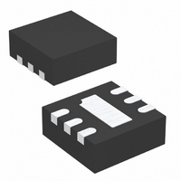
LTC3221EDC#TRPBF Linear Technology, LTC3221EDC#TRPBF Datasheet - Page 6

LTC3221EDC#TRPBF
Manufacturer Part Number
LTC3221EDC#TRPBF
Description
IC SW CAP/DBLR ADJ 60MA 6DFN
Manufacturer
Linear Technology
Type
Switched Capacitor (Charge Pump), Doublerr
Datasheet
1.LTC3221EDC-3.3TRMPBF.pdf
(12 pages)
Specifications of LTC3221EDC#TRPBF
Internal Switch(s)
Yes
Synchronous Rectifier
No
Number Of Outputs
1
Voltage - Output
Adjustable
Current - Output
60mA
Frequency - Switching
600kHz
Voltage - Input
1.8 ~ 5.5 V
Operating Temperature
-40°C ~ 85°C
Mounting Type
Surface Mount
Package / Case
6-DFN
Operating Supply Voltage (min)
1.8V
Operating Supply Voltage (max)
5.5V
Operating Temp Range
-40C to 85C
Operating Temperature Classification
Industrial
Pin Count
6
Mounting
Surface Mount
Lead Free Status / RoHS Status
Lead free / RoHS Compliant
Power - Output
-
Lead Free Status / Rohs Status
Compliant
Available stocks
Company
Part Number
Manufacturer
Quantity
Price
PI FU CTIO S
BLOCK DIAGRA
OPERATIO
The LTC3221 family uses a switched capacitor charge pump
to boost V
achieved by monitoring the output voltage, V
comparator (CMP in the Block Diagram) and keeping it
within a hysteresis window. If V
trip point of CMP, V
rent, I
goes above the upper trip point of CMP, or if the upper
trip point is not reached after 0.8µs, C
from V
to GND to allow I
0.8µs. After which, I
supply current low. CMP continues to monitor V
turns on I
LTC3221/
LTC3221-3.3/LTC3221-5
C+ (Pin 1): Flying Capacitor Positive Terminal.
C– (Pin 2): Flying Capacitor Negative Terminal.
⎯ S ⎯ H ⎯ D ⎯ N (Pin 3) (LTC3221-3.3/LTC3221-5): Active Low
Shutdown Input. A low on ⎯ S ⎯ H ⎯ D ⎯ N disables the LTC3221-3.3/
LTC3221-5. ⎯ S ⎯ H ⎯ D ⎯ N must not be allowed to fl oat.
FB (Pin 3) (LTC3221): Feedback. The voltage on this pin
is compared to the internal reference voltage (1.23V) by
the error comparator to keep the output in regulation. An
external resistor divider is required between V
to program the output voltage.
6
U
SW
OUT
in series with the fl ying capacitor C
SW
IN
. The bottom plate of C
U
SHDN
V
to a regulated output voltage. Regulation is
OUT
if the lower threshold is reached again.
6
3
U
SW
OUT
SW
U
to replenish the charge on C
+
–
(Refer to Block Diagrams)
V
is turned off to keep the operating
REF
is charged by the controlled cur-
CMP
LTC3221-3.3/LTC3221-5
W
OUT
CONTROL
FLY
drops below the lower
FLY
is then connected
is disconnected
FLY
2
OUT
. Once V
1
2
1
OUT
OUT
using a
and FB
FLY
I
SW
and
OUT
for
1
5
2
4
C
V
C
GND
+
IN
–
V
OUT
FB
Shutdown Mode
The ⎯ S ⎯ H ⎯ D ⎯ N pin is a CMOS input with a threshold voltage
of approximately 0.8V. The LTC3221-3.3/ LTC3221-5 are
in shutdown when a logic low is applied to the ⎯ S ⎯ H ⎯ D ⎯ N
pin. In shutdown mode, all circuitry is turned off and the
LTC3221-3.3/ LTC3221-5 draw only leakage current from
the V
V
input, it should never be allowed to fl oat.
When ⎯ S ⎯ H ⎯ D ⎯ N is asserted low, the charge pump is fi rst dis-
abled, but the LTC3221-3.3/LTC3221-5 continue to draw
5µA of supply current. This current will drop to zero when
the output voltage (V
GND (Pin 4): Ground. Should be tied to a ground plane
for best performance.
V
with a 2.2µF low ESR capacitor.
V
mance, V
low ESR capacitor as close as possible to the pin.
Exposed Pad (Pin 7) Ground. The exposed pad must be
soldered to PCB ground to provide electrical contact and
optimum thermal performance.
IN
IN
OUT
6
3
. Since the ⎯ S ⎯ H ⎯ D ⎯ N pin is a very high impedance CMOS
(Pin 5): Input Supply Voltage. V
IN
(Pin 6): Regulated Output Voltage. For best perfor-
supply. Furthermore, V
+
–
V
OUT
REF
CMP
should be bypassed with a 2.2µF or higher
LTC3221
CONTROL
OUT
) is fully discharged to 0V.
2
OUT
1
2
1
IN
is disconnected from
I
should be bypassed
SW
3221 BD
1
5
2
4
C
V
C
GND
+
IN
–
3221f


