LTC3221EDC#TRPBF Linear Technology, LTC3221EDC#TRPBF Datasheet

IC SW CAP/DBLR ADJ 60MA 6DFN

LTC3221EDC#TRPBF

Manufacturer Part Number
LTC3221EDC#TRPBF
Description
IC SW CAP/DBLR ADJ 60MA 6DFN
Manufacturer
Linear Technology
Type
Switched Capacitor (Charge Pump), Doublerr
Datasheet

Specifications of LTC3221EDC#TRPBF

Internal Switch(s)
Yes
Synchronous Rectifier
No
Number Of Outputs
1
Voltage - Output
Adjustable
Current - Output
60mA
Frequency - Switching
600kHz
Voltage - Input
1.8 ~ 5.5 V
Operating Temperature
-40°C ~ 85°C
Mounting Type
Surface Mount
Package / Case
6-DFN
Operating Supply Voltage (min)
1.8V
Operating Supply Voltage (max)
5.5V
Operating Temp Range
-40C to 85C
Operating Temperature Classification
Industrial
Pin Count
6
Mounting
Surface Mount
Lead Free Status / RoHS Status
Lead free / RoHS Compliant
Power - Output
-
Lead Free Status / Rohs Status
Compliant

Available stocks

Company
Part Number
Manufacturer
Quantity
Price
Company:
Part Number:
LTC3221EDC#TRPBFLTC3221EDC
Manufacturer:
LT
Quantity:
10 000
Company:
Part Number:
LTC3221EDC#TRPBFLTC3221EDC#PBF
Manufacturer:
LT
Quantity:
1 348
Company:
Part Number:
LTC3221EDC#TRPBFLTC3221EDC#PBF
Manufacturer:
LINEAR/凌特
Quantity:
20 000
Company:
Part Number:
LTC3221EDC#TRPBFLTC3221EDC#TRMPBF
Manufacturer:
ADI/亚德诺
Quantity:
20 000
Company:
Part Number:
LTC3221EDC#TRPBFLTC3221EDC-3.3
Manufacturer:
LT
Quantity:
10 000
FEATURES
APPLICATIO S
TYPICAL APPLICATIO
Ultralow Power: 8µA Quiescent Current
Regulated Output Voltages: 3.3V ±4%, 5V ±4%, ADJ
V
Output Current: Up to 60mA
No Inductors Needed
Very Low Shutdown Current: <1µA
Shutdown Disconnects Load from V
Burst Mode Control
Short-Circuit Protected
Solution Profi le < 1mm
Tiny 2mm × 2mm 6-Pin DFN Package
Low Power 2 AA Cell to 3.3V Supply
Memory Backup Supplies
Tire Pressure Sensors
General Purpose Low Power Li-Ion to 5V Supply
RF Transmitters
Glucose Meters
IN
1.8V to 4.4V (LTC3221-3.3)
2.7V to 5.5V (LTC3221-5)
Range:
REGULATED 3.3V OUTPUT FROM 1.8V TO 4.4V INPUT
REGULATED 5V OUTPUT FROM 2.7V TO 5.5V INPUT
2.2µF
OFF ON
V
IN
U
4,7
5
3
V
I
I
V
I
I
OUT
OUT
OUT
OUT
V
GND
SHDN
OUT
OUT
C
LTC3221-X
IN
2
= OmA TO 25mA; V
= OmA TO 60mA; V
= OmA TO 25mA; V
= OmA TO 60mA; V
1µF
= 3.3V ±4%
= 5V ±4%
V
OUT
C
+
1
6
3221 TA01
U
4.7µF
IN
IN
IN
IN
V
OUT
IN
>1.8V
>2V
>2.7V
>3V
DESCRIPTIO
The LTC
converters that produce a regulated output at up to 60mA.
The input voltage range is 1.8V to 5.5V. Extremely low
operating current (8µA typical at no load) and low external
parts count (one fl ying capacitor and two small bypass
capacitors at V
small, battery-powered applications.
The LTC3221 family includes fi xed 5V and 3.3V output
versions plus an adjustable version. All parts operate
as Burst Mode
to achieve ultralow quiescent current. The chips use a
controlled current to supply the output and will survive
a continuous short-circuit from V
of the adjustable LTC3221 can be used to program the
desired output voltage.
The LTC3221 family is available in a low profi le (0.75mm)
2mm × 2mm 6-pin DFN package.
Mode is a registered trademark of Linear Technology Corporation. All other trademarks are
the property of their respective owners.
Regulated Charge Pump
, LT, LTC and LTM are registered trademarks of Linear Technology Corporation. Burst
®
3221 family are micropower charge pump DC/DC
LTC3221-3.3/LTC3221-5
16
14
12
10
8
6
4
2
0
1.5
T
T
T
A
A
IN
A
= 25°C
= –45°C
®
= 90°C
2.0
and V
No-Load Input Current
switched capacitor voltage doublers
vs Supply Voltage
U
SUPPLY VOLTAGE (V)
2.5
OUT
3.0
) make them ideally suited for
Micropower,
3.5
in 2 × 2 DFN
OUT
4.0
to GND. The FB pin
3221 TA01b
LTC3221/
4.5
1
3221f

Related parts for LTC3221EDC#TRPBF

LTC3221EDC#TRPBF Summary of contents

Page 1

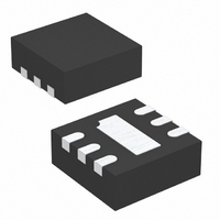
... The LTC3221 family is available in a low profi le (0.75mm) 2mm × 2mm 6-pin DFN package. , LT, LTC and LTM are registered trademarks of Linear Technology Corporation. Burst Mode is a registered trademark of Linear Technology Corporation. All other trademarks are the property of their respective owners. 16 ...

Page 2

LTC3221/ LTC3221-3.3/LTC3221 ABSOLUTE AXI U RATI GS (Note 1) , ⎯ S ⎯ H ⎯ D ⎯ ............................................. – 0. GND ............................................. – 0.3V to 5.5V OUT V ...

Page 3

ELECTRICAL CHARACTERISTICS temperature range, otherwise specifi cations are 1µ 2.2µ 2.2µF, unless otherwise specifi ed. FLY IN OUT SYMBOL PARAMETER LTC3221-3.3/LTC3221-5 I Shutdown Supply Current ⎯ S ⎯ H ⎯ D ⎯ ...

Page 4

LTC3221/ LTC3221-3.3/LTC3221 TYPICAL PERFOR A CE CHARACTERISTICS Load Regulation 3.36 3. 3.2V IN 3.32 3.30 3. 2.5V IN 3.26 3. 1.8V IN 3.22 3.20 3.18 3. 100 ...

Page 5

W U TYPICAL PERFOR A CE CHARACTERISTICS Load Regulation 5.10 5. 4. 3. 2.7V IN 4.90 4.85 4. 100 LOAD CURRENT (mA) 3221 G16 No-Load ...

Page 6

LTC3221/ LTC3221-3.3/LTC3221 CTIO S C+ (Pin 1): Flying Capacitor Positive Terminal. C– (Pin 2): Flying Capacitor Negative Terminal. ⎯ S ⎯ H ⎯ D ⎯ N (Pin 3) (LTC3221-3.3/LTC3221-5): Active Low Shutdown Input. A low ...

Page 7

U OPERATIO (Refer to Block Diagrams) The LTC3221 has a FB pin in place of the ⎯ S ⎯ H ⎯ D ⎯ N pin. This allows the output voltage to be programmed using an external resistive divider. Burst Mode ...

Page 8

LTC3221/ LTC3221-3.3/LTC3221 APPLICATIO S I FOR ATIO depends on many factors such as the oscillator frequency (f ), value of the fl ying capacitor (C OSC time, the internal switch resistances (R the external capacitors. A fi rst ...

Page 9

U U APPLICATIO S I FOR ATIO be expressed by the following equation – OUT ≡ ≅ MIN ( ) I f OUT OSC where f is the switching frequency (600kHz) and C OSC ...

Page 10

LTC3221/ LTC3221-3.3/LTC3221 APPLICATIO S I FOR ATIO If the standing current is too low, the FB pin becomes very sensitive to the switching noise and will result in errors in the programmed V . OUT The compensation capacitor ...

Page 11

... DRAWING NOT TO SCALE 3. ALL DIMENSIONS ARE IN MILLIMETERS Information furnished by Linear Technology Corporation is believed to be accurate and reliable. However, no responsibility is assumed for its use. Linear Technology Corporation makes no representation that the interconnection of its circuits as described herein will not infringe on existing patent rights Package 6-Lead Plastic DFN (2mm × ...

Page 12

... Buck/Boost Charge Pump, I Low Noise, 5V Output or Adjustable V : 2.7V to 5.5V, 3mm × 3mm DFN-10 Package 150mA (LTC3204-5 50mA (LTC3204-3. 150mA Output www.linear.com ● = 500µ 2.7V to 10V IN , 2.5V to 5.5V Output RMS = 60µ 2. 1006 • PRINTED IN USA © LINEAR TECHNOLOGY CORPORATION 2006 3221f ...

Related keywords