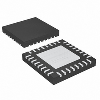
MAX5072ETJ+ Maxim Integrated Products, MAX5072ETJ+ Datasheet - Page 4

MAX5072ETJ+
Manufacturer Part Number
MAX5072ETJ+
Description
IC CONV BUCK/BOOST 32-TQFN
Manufacturer
Maxim Integrated Products
Type
Step-Down (Buck), Step-Up (Boost)r
Datasheet
1.MAX5072ETJ.pdf
(27 pages)
Specifications of MAX5072ETJ+
Internal Switch(s)
Yes
Synchronous Rectifier
No
Number Of Outputs
2
Voltage - Output
0.8 ~ 28 V
Current - Output
1A, 2A
Frequency - Switching
200kHz ~ 2.2MHz
Voltage - Input
4.5 ~ 23 V
Operating Temperature
-40°C ~ 85°C
Mounting Type
Surface Mount
Package / Case
32-TQFN Exposed Pad
Power - Output
2.76W
Output Voltage
5.2 V
Output Current
2 A
Input Voltage
5.5 V to 23 V
Supply Current
2.2 mA
Switching Frequency
1250 KHz
Mounting Style
SMD/SMT
Maximum Operating Temperature
+ 85 C
Minimum Operating Temperature
- 40 C
Lead Free Status / RoHS Status
Lead free / RoHS Compliant
2.2MHz, Dual-Output Buck or Boost
Converter with POR and Power-Fail Output
ELECTRICAL CHARACTERISTICS (continued)
(V+ = VL = 5.2V or V+ = 5.5V to 23V, EN_ = VL, SYNC = GND, I
R
4
INTERNAL OSCILLATOR/SYNC
Maximum Duty Cycle
Switching Frequency Range
Switching Frequency
Switching Frequency Accuracy
SYNC Frequency Range
SYNC High Threshold
SYNC Low Threshold
SYNC Input MIN Pulse Width
Clock Output Phase Delay
SYNC to SOURCE 1 Phase Delay
Clock Output High Level
Clock Output Low Level
FSEL1
FSEL1 Input High Threshold
FSEL1 Input Low Threshold
EN_ INPUTS
EN_ Input High Threshold
EN_ Input Low Threshold
EN_ Bias Current
MANUAL RESET (MR) AND POWER-ON-RESET (RST)
MR Minimum Pulse Width
MR Glitch Immunity
MR to RST Propagation Delay
MR Input High Threshold
MR Input Low Threshold
MR Internal Pullup Resistor
Power-On-Reset Threshold
FB_ to RST Propagation Delay
RST Active Timeout Period
RST Output Voltage
RST Output Leakage Current
OSC
_______________________________________________________________________________________
= 10kΩ (circuit of Figure 1), T
PARAMETER
A
SYNC
V
= T
V
SYMBOL
CLKOUT
V
V
t
CLKOUTH
PHASE
CLKOUTL
I
SYNCIN
D
f
I
V
RSTLK
SYNCH
SYNCL
SYNC
B(EN)
R
f
t
V
J
f
V
V
t
V
V
V
V
t
t
RST_
SET
MAX
MD
SW
MR
FD
RP
MR
TH
IH
IH
IH
= T
PHASE
IL
IL
IL
MIN
to T
SYNC = SGND, f
SYNC = SGND, f
Each converter
R
5.6kΩ
SYNC input frequency is twice the
individual converter frequency
ROSC = 60kΩ, 1%, with respect to
converter 2/SOURCE2 waveform
ROSC = 60kΩ, 1%
VL = 5.2V, sourcing 5mA
VL = 5.2V, sinking 5mA
V+ = VL = +5.2V
V+ = VL = +5.2V
V+ = VL = +5.2V
V+ = VL = +5.2V
Maximum glitch pulse width allowed for
RST to remain high
V+ = VL = +5.2V
V+ = VL = +5.2V
RST goes high 180ms after V
V
FB overdrive from 0.8V to 0.6V
I
I
V+ = VL = 5.2V, V
SINK
SINK
OSC
OUT2
MAX
= 3mA (MAX5072ETJ)
= 3mA (MAX5072ATJ)
= 10kΩ, each converter
≤
, unless otherwise noted.) (Note 1)
cross this threshold
R
OSC ≤
CONDITIONS
VL
56kΩ, 1%, each converter
SW
SW
= 0, PGND = SGND, C
RST
= 1.25MHz
= 2.2MHz
= 23V, V
OUT1
FB
_ = 0.8V
and
BYPASS
1125
MIN
200
400
140
-15
2.4
2.4
2.4
2.4
84
84
90
4
= 0.22µF, C
1250
TYP
92.5
100
100
200
1.8
1.2
1.1
86
86
45
45
44
1
VL
= 4.7µF (ceramic),
MAX
2200
1375
4400
0.52
+15
250
360
0.8
0.4
0.8
0.8
0.8
0.4
95
95
10
95
1
degrees
degrees
% V
UNITS
kHz
kHz
kHz
kΩ
ms
nA
µA
ns
µs
ns
µs
µs
%
%
V
V
V
V
V
V
V
V
V
V
V
OUT


