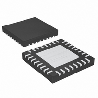
MAX5072ETJ+ Maxim Integrated Products, MAX5072ETJ+ Datasheet - Page 2

MAX5072ETJ+
Manufacturer Part Number
MAX5072ETJ+
Description
IC CONV BUCK/BOOST 32-TQFN
Manufacturer
Maxim Integrated Products
Type
Step-Down (Buck), Step-Up (Boost)r
Datasheet
1.MAX5072ETJ.pdf
(27 pages)
Specifications of MAX5072ETJ+
Internal Switch(s)
Yes
Synchronous Rectifier
No
Number Of Outputs
2
Voltage - Output
0.8 ~ 28 V
Current - Output
1A, 2A
Frequency - Switching
200kHz ~ 2.2MHz
Voltage - Input
4.5 ~ 23 V
Operating Temperature
-40°C ~ 85°C
Mounting Type
Surface Mount
Package / Case
32-TQFN Exposed Pad
Power - Output
2.76W
Output Voltage
5.2 V
Output Current
2 A
Input Voltage
5.5 V to 23 V
Supply Current
2.2 mA
Switching Frequency
1250 KHz
Mounting Style
SMD/SMT
Maximum Operating Temperature
+ 85 C
Minimum Operating Temperature
- 40 C
Lead Free Status / RoHS Status
Lead free / RoHS Compliant
ABSOLUTE MAXIMUM RATINGS
V+ to PGND............................................................-0.3V to +25V
SGND to PGND .....................................................-0.3V to +0.3V
VL to SGND...................-0.3V to the lower of +6V or (V+ + 0.3V)
BST1/VDD1, BST2/VDD2, DRAIN_, PFO,
BST1/VDD1 to SOURCE1,
SOURCE_ to SGND................................................-0.6V to +25V
EN_ to SGND ................................................-0.3V to (VL + 0.3V)
CLKOUT, BYPASS, OSC, FSEL1, COMP1,
SOURCE1, DRAIN1 Peak Current ..............................5A for 1ms
2.2MHz, Dual-Output Buck or Boost
Converter with POR and Power-Fail Output
Stresses beyond those listed under “Absolute Maximum Ratings” may cause permanent damage to the device. These are stress ratings only, and functional
operation of the device at these or any other conditions beyond those indicated in the operational sections of the specifications is not implied. Exposure to
absolute maximum rating conditions for extended periods may affect device reliability.
ELECTRICAL CHARACTERISTICS
(V+ = VL = 5.2V or V+ = 5.5V to 23V, EN_ = VL, SYNC = GND, I
R
2
SYSTEM SPECIFICATIONS
Input Voltage Range
Operating Supply Current
V+ Standby Supply Current
Efficiency
STARTUP/VL REGULATOR
VL Undervoltage Lockout Trip
Level
VL Undervoltage Lockout
Hysteresis
VL Output Voltage
BYPASS OUTPUT
BYPASS Voltage
BYPASS Load Regulation
SOFT-START
Digital Ramp Period
Soft-Start Steps
OSC
SGND .................................................................-0.3V to +30V
BST2/VDD2 to SOURCE2 ....................................-0.3V to +6V
COMP2, PFI, MR, SYNC, FB_ to SGND....-0.3V to (VL + 0.3V)
_______________________________________________________________________________________
= 10kΩ (circuit of Figure 1), T
PARAMETER
A
∆V
= T
SYMBOL
V
UVLO
BYPASS
I
BYPASS
STBY
RST, PGOOD1 to
J
V+
VL
I
η
Q
= T
MIN
to T
(Note 2)
VL = V+
VL unloaded, no switching,
V
EN_ = 0, MR, PFO, and PGOOD_ floating,
V+ = 12V, R
EN_ = 0, MR, PFO, and PGOOD_ floating,
V+ = 12V, R
V
V
(f
VL falling
V+ = 5.5V to 23V, I
I
I
0
Internal 6-bit DAC
BYPASS
BYPASS
FB_
OUT1
OUT2
SW
≤
I
MAX
BYPASS ≤
= 1.25MHz)
= 1V, V+ = 12V, R
= 3.3V at 1.5A,
= 2.5V at 0.75A
, unless otherwise noted.) (Note 1)
= 0, R
= 0, R
OSC
OSC
50µA, R
OSC
OSC
CONDITIONS
VL
= 60kΩ (MAX5072ETJ)
= 60kΩ (MAX5072ATJ)
= 0, PGND = SGND, C
SOURCE
= 60kΩ (MAX5072ETJ)
= 60kΩ (MAX5072ATJ)
SOURCE2, DRAIN2 Peak Current ..............................3A for 1ms
VL, BYPASS to SGND Short Circuit............................Continuous
Continuous Power Dissipation (T
Package Junction-to-Case Thermal Resistance (θJ
Operating Temperature Ranges:
Junction Temperature ......................................................+150°C
Storage Temperature Range .............................-65°C to +150°C
Lead Temperature (soldering, 10s) .................................+300°C
*As per JEDEC51 standard.
OSC
32-Pin Thin QFN (derate 21.3mW/°C above +70°C).....2758mW*
MAX5072ETJ (T
MAX5072ATJ (T
OSC
= 60kΩ
= 0 to 40mA
= 60kΩ
V+ = VL = 5V
V+ = 12V
V+ = 16V
MIN
MIN
BYPASS
to T
to T
MAX
MAX
1.975
MIN
3.95
1.98
5.5
4.5
4.9
0
= 0.22µF, C
)...........................-40°C to +85°C
).........................-40°C to +125°C
A
= +70°C)
2048
TYP
2.00
2.00
175
2.2
0.6
0.6
4.1
5.2
82
80
78
64
2
VL
= 4.7µF (ceramic),
2.025
MAX
4.25
2.02
5.5
1.2
1.4
1.4
5.5
23
10
C
).......2°C/W
UNITS
cycles
clock
steps
f
mA
mA
mV
mV
OSC
%
V
V
V
V


