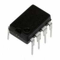
LM2578AN/NOPB National Semiconductor, LM2578AN/NOPB Datasheet - Page 4

LM2578AN/NOPB
Manufacturer Part Number
LM2578AN/NOPB
Description
IC REG SIMPLE SWITCHER 8-DIP
Manufacturer
National Semiconductor
Type
Step-Down (Buck), Step-Up (Boost), Inverting, Flybackr
Datasheet
1.LM3578AMNOPB.pdf
(20 pages)
Specifications of LM2578AN/NOPB
Internal Switch(s)
Yes
Synchronous Rectifier
No
Number Of Outputs
1
Current - Output
750mA
Frequency - Switching
20kHz
Voltage - Input
2 ~ 40 V
Operating Temperature
-40°C ~ 85°C
Mounting Type
Through Hole
Package / Case
8-DIP (0.300", 7.62mm)
No. Of Outputs
1
Output Voltage
1V
Output Current
750mA
No. Of Pins
8
Operating Temperature Range
-40°C To +85°C
Msl
MSL 1 - Unlimited
Input Voltage
40V
Input Voltage Primary Max
40V
Rohs Compliant
Yes
Primary Input Voltage
40V
Lead Free Status / RoHS Status
Lead free / RoHS Compliant
Voltage - Output
-
Power - Output
-
Other names
*LM2578AN
*LM2578AN/NOPB
LM2578AN
*LM2578AN/NOPB
LM2578AN
www.national.com
CURRENT LIMIT
∆V
I
DEVICE POWER CONSUMPTION
I
CL
S
Electrical Characteristics
Note 1: Absolute Maximum Ratings indicate limits beyond which damage to the device may occur. DC and AC electrical specifications do not apply when operating
the device beyond its rated operating conditions.
Note 2: For T
Note 3: At elevated temperatures, devices must be derated based on package thermal resistance. The device in the 8-pin DIP must be derated at 95˚C/W, junction
to ambient. The device in the surface-mount package must be derated at 150˚C/W, junction-to-ambient.
Note 4: Human body model, 1.5 kΩ in series with 100 pF.
Note 5: Typical values are for T
Note 6: All limits guaranteed at room temperature (standard type face) and at temperature extremes (bold type face). Room temperature limits are 100% production
tested. Limits at temperature extremes are guaranteed via correlation using standard Statistical Quality Control (SQC) methods. All limits are used to calculate
AOQL.
Note 7: Input terminals are protected from accidental shorts to ground but if external voltages higher than the reference voltage are applied, excessive current will
flow and should be limited to less than 5 mA.
Note 8: I
Note 9: Connection of a 10 kΩ resistor from pin 1 to pin 4 will drive the duty cycle to its maximum, typically 90%. Applying the minimum Current Limit Sense Voltage
to pin 7 will not reduce the duty cycle to less than 50%. Applying the maximum Current Limit Sense Voltage to pin 7 is certain to reduce the duty cycle below 50%.
Increasing this voltage by 15 mV may be required to reduce the duty cycle to 0%, when the Collector output swing is 40V or greater (see Ground-Referred Current
Limit Sense Voltage typical curve).
Typical Performance Characteristics
Symbol
These specifications apply for 2V ≤ V
duty cycle ≤ 75%, unless otherwise specified. Values in standard typeface are for T
operation over the specified operating junction temperature range.
CL
/∆T
1
and I
J
Sense Voltage Temperature Drift
Sense Bias Current
Supply Current
≥ 100˚C, the Emitter pin voltage should not be driven more than 0.6V below ground (see Application Information).
2
are the external sink currents at the inputs (refer to Test Circuit).
Oscillator Frequency Change
with Temperature
Parameter
J
= 25˚C and represent the most likely parametric norm.
IN
≤ 40V (2.2V ≤ V
(Continued)
00871132
Referred to V
Referred to ground
Output OFF, V
Output ON, I
V
E
= 0V
IN
≤ 40V for T
Conditions
C
4
IN
E
= 750 mA pulsed,
= 0V
J
≤ −25˚C), timing capacitor C
Oscillator Voltage Swing
J
= 25˚C; values in boldface type apply for
(Note 5)
Typical
0.3
4.0
0.4
2.0
14
Limit (Note 6)
T
LM2578A/
LM3578A
= 3900 pF, and 25% ≤
3.5/4.0
00871133
%/˚C
µA
µA
mA
mA (max)
mA
Units


