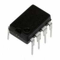
LM2578AN/NOPB National Semiconductor, LM2578AN/NOPB Datasheet - Page 16

LM2578AN/NOPB
Manufacturer Part Number
LM2578AN/NOPB
Description
IC REG SIMPLE SWITCHER 8-DIP
Manufacturer
National Semiconductor
Type
Step-Down (Buck), Step-Up (Boost), Inverting, Flybackr
Datasheet
1.LM3578AMNOPB.pdf
(20 pages)
Specifications of LM2578AN/NOPB
Internal Switch(s)
Yes
Synchronous Rectifier
No
Number Of Outputs
1
Current - Output
750mA
Frequency - Switching
20kHz
Voltage - Input
2 ~ 40 V
Operating Temperature
-40°C ~ 85°C
Mounting Type
Through Hole
Package / Case
8-DIP (0.300", 7.62mm)
No. Of Outputs
1
Output Voltage
1V
Output Current
750mA
No. Of Pins
8
Operating Temperature Range
-40°C To +85°C
Msl
MSL 1 - Unlimited
Input Voltage
40V
Input Voltage Primary Max
40V
Rohs Compliant
Yes
Primary Input Voltage
40V
Lead Free Status / RoHS Status
Lead free / RoHS Compliant
Voltage - Output
-
Power - Output
-
Other names
*LM2578AN
*LM2578AN/NOPB
LM2578AN
*LM2578AN/NOPB
LM2578AN
www.national.com
Typical Applications
D1 is a Schottky type diode such as a 1N5818 or 1N5819.
L1 is found as described in the buck converter section, using
the inductance chart for Figure 16 for the boost configuration
and 20% discontinuity.
INVERTING REGULATOR
Figure 20 shows the basic configuration for an inverting
regulator. The input voltage is of a positive polarity, but the
output is negative. The output may be less than, equal to, or
greater in magnitude than the input. The relationship be-
tween the magnitude of the input voltage and the output
voltage is V
BUCK-BOOST REGULATOR
The Buck-Boost Regulator, shown in Figure 22, may step a
voltage up or down, depending upon whether or not the
desired output voltage is greater or less than the input
voltage. In this case, the output voltage is 12V with an input
voltage from 9V to 15V. The circuit exhibits an efficiency of
75%, with a load regulation of 60 mV (10 mA to 100 mA) and
a line regulation of 52 mV.
R1 = (V
R3 = V/0. 75A
R4, C1, C3 and C4 are defined in the “Boost Regulator”
section.
V
V
V
I
I
o
min
o
in
o
ripple
= 300 mA
FIGURE 20. Basic Inverting Regulator
− 1) R2 where R2 = 10 kΩ
= −15V
= 5V
= 60 mA
o
= 5 mV
= V
in
x (t
on
/t
off
).
R4 = 190Ω
R5 = 82Ω
R6 = 220 kΩ
C1 = 1820 pF
C2 = 1000 µF
(Continued)
00871110
FIGURE 21. Inverting Regulator
16
Figure 21 shows an LM2578A configured as a 5V to −15V
polarity inverter with an output current of 300 mA, a load
regulation of 44 mV (60 mA to 300 mA) and a line regulation
of 50 mV (4.5V ≤ V
where:
V, V
Boosted Output Current” section.
∆I
R5 is defined in the “Buck with Boosted Output Current”
section.
R6 serves the same purpose as R4 in the Boost Regulator
circuit and is typically 220 kΩ.
C1, C3 and C4 are defined in the “Boost Regulator” section.
L1 is found as outlined in the section on buck converters,
using the inductance chart of Figure 16 for the invert con-
figuration and 20% discontinuity.
D1 and D2 are Schottky type diodes such as the 1N5818 or
1N5819.
where:
V
V
tor.
V
d
sat
sat1
L
is the forward voltage drop of the diodes.
= 2(I
BE1
is the saturation voltage of the LM2578A output transis-
is the saturation voltage of transistor Q1.
f
R1 = 160 kΩ
R2 = 10 kΩ
R3 = 0.01Ω
, V
osc
LOAD(min)
sat
R1 = (|V
= 50 kHz
R4 = 10V
, and B
C2 ≥ I
L1 ≥ (V
R3 = V/(I
)(V
o
o
in
f
in
| +1) R2 where R2 = 10 kΩ.
are defined in the “Buck Converter with
|V
BE1
≤ 8.5V).
in
+|V
o
|/[f
− V
00871112
B
L(max, DC)
f
o
/(I
osc
|)/V
sat
L (max, DC)
(|V
IN
C3 = 20 pF
C4 = 0.0022 µF
L1 = 150 µH
D1 = 1N5818
− V
o
| + V
+ 0.5 ∆I
sat1
) (t
in
+ 0.5 ∆I
) V
on
ripple
L
/I
).
p
)
]
L
)


