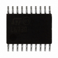
L6730 STMicroelectronics, L6730 Datasheet - Page 27

L6730
Manufacturer Part Number
L6730
Description
IC CTRLR ADJ STPDN SYNC 20-TSSOP
Manufacturer
STMicroelectronics
Type
Step-Down (Buck)r
Datasheet
1.L6730TR.pdf
(52 pages)
Specifications of L6730
Internal Switch(s)
No
Synchronous Rectifier
Yes
Number Of Outputs
1
Voltage - Output
Adj to 0.6V
Frequency - Switching
100kHz ~ 1MHz
Voltage - Input
1.8 ~ 14 V
Operating Temperature
-40°C ~ 85°C
Mounting Type
Surface Mount
Package / Case
20-TSSOP Exposed Pad, 20-eTSSOP, 20-HTSSOP
Output Voltage
0.6 V
Input Voltage
1.8 V to 14 V
Mounting Style
SMD/SMT
Maximum Operating Temperature
+ 85 C
Minimum Operating Temperature
- 40 C
For Use With
497-5868 - EVAL BOARD 30A 400KHZ L6730497-5501 - EVAL BOARD FOR L6730XX
Lead Free Status / RoHS Status
Lead free / RoHS Compliant
Current - Output
-
Power - Output
-
Lead Free Status / Rohs Status
Lead free / RoHS Compliant
Other names
497-5291-5
Available stocks
Company
Part Number
Manufacturer
Quantity
Price
Company:
Part Number:
L6730BTR
Manufacturer:
STM
Quantity:
3 172
Company:
Part Number:
L6730DTR
Manufacturer:
PH
Quantity:
4 199
Part Number:
L6730TR
Manufacturer:
ST
Quantity:
20 000
L6730 - L6730B
5.9
5.10
Working with a 12 V BUS, setting the UVLO at 8.6 V can be very helpful to limit the input
current in case of BUS fall.
Figure 22. Valley OCP (L6730B)
Adjustable masking time
By connecting the masking time pin to V
values for the peak current protection leading edge blanking time. This is useful to avoid any
false OCP trigger due to spikes and oscillations generated at the turn-on of the high-side
MOSFET(s). The amount of this noise depends very much on the layout, MOSFETs, free-
wheeling diode, switched current, and input voltage.
When good layout and medium current are used, the minimum masking time can be
chosen, while in case of higher noise, it is better to select the maximum masking time. By
connecting the t
GND results in about 260 ns masking time.
Multifunction pin (S/O/U L6730) (CC/O/U L6730B)
With this pin it is possible:
●
●
●
I
To enable disable the sink mode current capability (L6730) or the constant current
protection (L6730B) at the end of the soft-start
To enable or disable the latch-mode for the OVP
To set the UVLO threshold for 5 V BUS and 12 V busses
L
V
OUT
MASK
T
OFF
pin to V
CCDR
Doc ID 11938 Rev 3
the masking time is about 400 ns, while connecting it to
CCDR
or GND it is possible to select two different
T
OFF
Valley th
Device description
27/52


