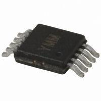
MIC2174-1YMM Micrel Inc, MIC2174-1YMM Datasheet - Page 21

MIC2174-1YMM
Manufacturer Part Number
MIC2174-1YMM
Description
IC BUCK SYNC ADJ 25A 10MSOP
Manufacturer
Micrel Inc
Series
Hyper Speed Control™r
Type
Step-Down (Buck)r
Datasheet
1.MIC2174-1YMM.pdf
(27 pages)
Specifications of MIC2174-1YMM
Internal Switch(s)
No
Synchronous Rectifier
Yes
Number Of Outputs
1
Voltage - Output
0.8 ~ 5.5 V
Frequency - Switching
300kHz
Voltage - Input
3 ~ 5.5 V
Operating Temperature
-40°C ~ 125°C
Mounting Type
Surface Mount
Package / Case
10-MSOP, Micro10™, 10-uMAX, 10-uSOP
Power - Output
421mW
Primary Input Voltage
40V
No. Of Outputs
2
Output Current
25A
Voltage Regulator Case Style
MSOP
No. Of Pins
10
Operating Temperature Range
-40°C To +125°C
Svhc
No SVHC (15-Dec-2010)
Lead Free Status / RoHS Status
Lead free / RoHS Compliant
Current - Output
-
Lead Free Status / RoHS Status
Lead free / RoHS Compliant, Lead free / RoHS Compliant
Other names
576-3546-5
Available stocks
Company
Part Number
Manufacturer
Quantity
Price
Company:
Part Number:
MIC2174-1YMM
Manufacturer:
Micrel Inc
Quantity:
135
Micrel, Inc.
PCB Layout Guidelines
Warning!!! To minimize EMI and output noise, follow
these layout recommendations.
PCB Layout is critical to achieve reliable, stable and
efficient performance. A ground plane is required to
control EMI and minimize the inductance in power,
signal and return paths.
The following guidelines should be followed to insure
proper operation of the MIC2174/MIC2174C converter.
IC
•
•
•
•
Input Capacitor
•
•
•
•
•
•
•
•
•
September 2010
The 2.2µF ceramic capacitor, which connects to the
V
terminal is very noise sensitive and placement of the
capacitor is very critical. Use wide traces to connect
to the IN and PGND pins.
Place the IC and MOSFETs close to the point of
load (POL).
Use fat traces to route the input and output power
lines.
Signal and power grounds should be kept separate
and connected at only one location.
Place the HSD input capacitor next.
Place the HSD input capacitors on the same side of
the board and as close to the MOSFETs as
possible.
Keep both the HSD and PGND connections short.
Place several vias to the ground plane close to the
HSD input capacitor ground terminal.
Use either X7R or X5R dielectric input capacitors.
Do not use Y5V or Z5U type capacitors.
Do not replace the ceramic input capacitor with any
other type of capacitor. Any type of capacitor can be
placed in parallel with the input capacitor.
If a Tantalum input capacitor is placed in parallel
with the input capacitor, it must be recommended for
switching regulator applications and the operating
voltage must be derated by 50%.
In “Hot-Plug” applications, a Tantalum or Electrolytic
bypass capacitor must be used to limit the over-
voltage spike seen on the input supply with power is
suddenly applied.
An additional Tantalum or Electrolytic bypass input
capacitor of 22µF or higher is required at the input
power connection.
IN
terminal, must be located right at the IC. The V
IN
21
Inductor
•
•
•
•
•
Output Capacitor
•
•
•
Schottky Diode (Optional)
•
•
•
RC Snubber
•
MOSFETs
•
•
•
•
Keep the inductor connection to the switch node
(LX) short.
Do not route any digital lines underneath or close to
the inductor.
Keep the switch node (LX) away from the feedback
(FB) pin.
The LX pin should be connected directly to the drain
of the low-side MOSFET to accurate sense the
voltage across the low-side MOSFET.
To minimize noise, place a ground plane underneath
the inductor.
Use a wide trace to connect the output capacitor
ground terminal to the input capacitor ground
terminal.
Phase margin will change as the output capacitor
value and ESR changes. Contact the factory if the
output capacitor is different from what is shown in
the BOM.
The feedback trace should be separate from the
power trace and connected as close as possible to
the output capacitor. Sensing a long high current
load trace can degrade the DC load regulation.
Place the Schottky diode on the same side of the
board as the MOSFETs and HSD input capacitor.
The connection from the Schottky diode’s Anode to
the input capacitors ground terminal must be as
short as possible.
The diode’s cathode connection to the switch node
(LX) must be keep as short as possible.
Place the RC snubber on the same side of the board
and as close to the MOSFETs as possible.
Low-side MOSFET gate drive trace (DL pin to
MOSFET gate pin) must be short and routed over a
ground plane. The ground plane should be the
connection between the MOSFET source and PGND.
Chose a low-side MOSFET with a high C
and a low internal gate resistance to minimize the
effect of dv/dt inducted turn-on.
Do not put a resistor between the LSD output and
the gate.
Use a 4.5V V
threshold voltage is more immune to glitches than a
2.5V or 3.3V rated MOSFET. MOSFETs that are
rated for operation at less than 4.5V V
be used.
GS
rated MOSFET. Its higher gate
MIC2174/MIC2174C
M9999-091310-C
GS
GS
should not
/C
GD
ratio


