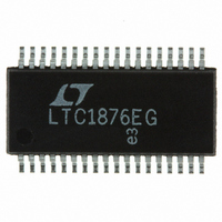
LTC1876EG#PBF Linear Technology, LTC1876EG#PBF Datasheet - Page 31

LTC1876EG#PBF
Manufacturer Part Number
LTC1876EG#PBF
Description
IC CTLR/REG STEP UP/DOWN 36SSOP
Manufacturer
Linear Technology
Series
PolyPhase®r
Type
Step-Down (Buck), Step-Up (Boost)r
Datasheet
1.LTC1876EGPBF.pdf
(36 pages)
Specifications of LTC1876EG#PBF
Internal Switch(s)
No
Synchronous Rectifier
Yes
Number Of Outputs
3
Voltage - Output
Adj to 34V
Current - Output
1A
Frequency - Switching
140kHz ~ 340kHz
Voltage - Input
3.5 ~ 36 V
Operating Temperature
-40°C ~ 85°C
Mounting Type
Surface Mount
Package / Case
36-SSOP
Primary Input Voltage
36V
No. Of Outputs
3
Output Voltage
36V
Output Current
25A
No. Of Pins
36
Operating Temperature Range
-40°C To +85°C
Msl
MSL 1 - Unlimited
Rohs Compliant
Yes
Lead Free Status / RoHS Status
Lead free / RoHS Compliant
Power - Output
-
Available stocks
Company
Part Number
Manufacturer
Quantity
Price
APPLICATIO S I FOR ATIO
signal ground pin and the ground return of C
return to the combined C
tor circuitry, are the signal and power grounds kept
separate? The regulator signal ground pin must return to
the C
3. Does the path formed by the top N-Channel MOSFET
Schottky diode (D1, D2) and the C
leads and PC trace lengths? The output capacitor (–)
plates should be connected as close as possible to the
(–) plates of the input capacitor by placing the capacitors
next to each other and away from the Schottky loop
described above. Also, the path formed by the AUXSW
pins, Schottky diode (D3) and the C
have short leads and PC trace lengths. The C
tor (–) plates should be connected as close as possible to
AUXIN
(–) plates.
R
IN
V
IN
C
U
IN
BOLD LINES INDICATE
HIGH, SWITCHING
CURRENT LINES.
KEEP LINES TO A
MINIMUM LENGTH.
+
OUT
U
(–) plates. Within the regula-
IN
OUT3
W
capacitor have short
capacitor should
Figure 16. Branch Current Waveforms
AUXIN
SW1
SW2
INTVCC
U
D1
D2
capaci-
must
the (–) plates of the C
capacitors next to each other and away from the D3 loop
described above.
4. If the input supply to the boost regulator is obtain from
one of the other outputs, is this connection short (< 1cm)?
5. Do the LTC1876 V
dividers connect to the (+) plates of its respective C
The resistive divider must be connected between the (+)
plate of C
decoupling capacitor should be as close as possible to the
LTC1876 SGND pin. A feedforward capacitor across R8
can be connected to enhance the transient response of the
boost regulator. The R2, R4 and R8 connections should
not be along the high current input feeds from the input
capacitor(s).
L1
L2
R
R
SENSE1
SENSE2
OUT
C
C
OUT1
OUT2
and signal ground and a small V
V
V
+
+
OUT1
OUT2
OSENSE
OUT3
and AUXV
(–) plates by placing the
1876 F16
R
R
LTC1876
L1
L2
FB
pins resistive
31
OSENSE
OUT
1876fa
?


