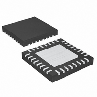
MAX8833ETJ+ Maxim Integrated Products, MAX8833ETJ+ Datasheet - Page 15

MAX8833ETJ+
Manufacturer Part Number
MAX8833ETJ+
Description
IC REG STP DWN DUAL 3A 32-TQFN
Manufacturer
Maxim Integrated Products
Type
Step-Down (Buck)r
Datasheet
1.MAX8833ETJ.pdf
(20 pages)
Specifications of MAX8833ETJ+
Internal Switch(s)
Yes
Synchronous Rectifier
No
Number Of Outputs
2
Voltage - Output
0.6 ~ 3.24 V
Current - Output
3A
Frequency - Switching
500kHz ~ 2MHz
Voltage - Input
2.35 ~ 3.6 V
Operating Temperature
-40°C ~ 85°C
Mounting Type
Surface Mount
Package / Case
32-TQFN Exposed Pad
Power - Output
2.76W
Output Voltage
0.6 V to 0.9 V
Output Current
3 A
Input Voltage
2.35 V to 3.6 V
Switching Frequency
2 MHz
Operating Temperature Range
- 40 C to + 85 C
Mounting Style
SMD/SMT
Duty Cycle (max)
95 %
Lead Free Status / RoHS Status
Lead free / RoHS Compliant
These equations are based on the assumptions that C9
>> C10, and R4 >> R8, which are true in most applica-
tions. Placement of these poles and zeros is deter-
mined by the frequencies of the double pole and ESR
zero of the power stage transfer function. It is also a
function of the desired closed-loop bandwidth. Figure 5
shows the pole zero cancellations in the type III com-
pensation design.
The following section outlines the step-by-step design
procedure to calculate the required compensation com-
ponents. Begin by setting the desired output voltage as
described in the Setting the Output Voltage section.
The crossover frequency f
bandwidth of the regulator) should be between 10%
and 20% of the switching frequency, f
crossover frequency results in a faster transient
response. Too high of a crossover frequency can result
in instability. Once f
farads) from the following equation:
Figure 5. Pole Zero Cancellations in Compensation Design
f
f
f
P
P
Z
______________________________________________________________________________________
2
3
2
_
_
_
EA
EA
EA
C
=
=
=
is chosen, calculate C9 (in
2
2
2
Dual, 3A, 2MHz Step-Down Regulator
C
π
π
π
POWER-STAGE TRANSFER FUNCTION
×
×
×
(or closed-loop, unity-gain
COMPENSATION TRANSFER FUNCTION
R
R
R
1
7
1
8
1
4
×
×
×
C
C
C
10
11
11
S
. A higher
DOUBLE POLES
FIRST AND SECOND ZEROS
FREQUENCY
where V
crossover frequency in Hertz, R4 is the upper feedback
resistor (in ohms), R
tance and the internal switch on-resistance, and R
the output load resistance (V
Due to the underdamped nature of the output LC double
pole, set the two zero frequencies of the type III com-
pensation less than the LC double-pole frequency to
provide adequate phase boost. Set the two zero fre-
quencies to 80% of the LC double-pole frequency.
Hence:
Set the third compensation pole, f
which yields:
C
IN
R
7
11
is the input voltage in volts, f
=
=
0 8
C
0 8
.
SECOND POLE
9
OPEN-LOOP GAIN
.
1
×
=
1
×
C
2
R
R
L
9
π
4
8
×
is the sum of the inductor resis-
×
=
×
THIRD POLE
f
C
C
L C
2 5
×
L C
O
.
×
R
C
×
OUT
×
4
11
×
ESR
O
×
V
O
R
R
IN
⎛
⎜
⎝
/I
×
L
1
×
L
OUT
(
+
+
R
(
+
R
R
R
O
R
R
O
P3_EA
O
).
O
L
O
+
+
⎞
⎟
⎠
ESR
ESR
, at f
)
)
C
Z_ESR
is the
O
15
is
,


