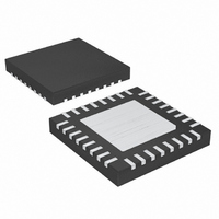
MAX8833ETJ+ Maxim Integrated Products, MAX8833ETJ+ Datasheet - Page 12

MAX8833ETJ+
Manufacturer Part Number
MAX8833ETJ+
Description
IC REG STP DWN DUAL 3A 32-TQFN
Manufacturer
Maxim Integrated Products
Type
Step-Down (Buck)r
Datasheet
1.MAX8833ETJ.pdf
(20 pages)
Specifications of MAX8833ETJ+
Internal Switch(s)
Yes
Synchronous Rectifier
No
Number Of Outputs
2
Voltage - Output
0.6 ~ 3.24 V
Current - Output
3A
Frequency - Switching
500kHz ~ 2MHz
Voltage - Input
2.35 ~ 3.6 V
Operating Temperature
-40°C ~ 85°C
Mounting Type
Surface Mount
Package / Case
32-TQFN Exposed Pad
Power - Output
2.76W
Output Voltage
0.6 V to 0.9 V
Output Current
3 A
Input Voltage
2.35 V to 3.6 V
Switching Frequency
2 MHz
Operating Temperature Range
- 40 C to + 85 C
Mounting Style
SMD/SMT
Duty Cycle (max)
95 %
Lead Free Status / RoHS Status
Lead free / RoHS Compliant
Dual, 3A, 2MHz Step-Down Regulator
In Figure 3d, EN1 and EN2 are connected together and
driven as a single input. Although both outputs begin
ramping up at the same time, slope matching is
achieved by selecting the SS_ capacitors. See the
Setting the Soft-Start Time section for information on
selecting the SS_ capacitors. In Figure 3d, the slope of
the output voltages during soft-start is equal. This is
achieved by setting the ratio of the soft-start capacitors
equal to the ratio of the output voltages:
The MAX8833 operates from 500kHz to 2MHz using
either its internal oscillator, or an externally supplied
clock. See the Setting the Switching Frequency section.
Thermal-overload protection limits the total power dissi-
pation of the MAX8833. Internal thermal sensors monitor
the junction temperature at each of the regulators. When
the junction temperature exceeds +165°C, the corre-
sponding regulator is shut down, allowing the IC to cool.
The thermal sensor turns the regulator on after the junc-
tion temperature cools by +20°C. In a continuous ther-
mal-overload condition, this results in a pulsed output.
Figure 3d. Startup and Sequencing Options—Matching Startup Slopes of Output Voltages with Internal Reference
12
______________________________________________________________________________________
Thermal-Overload Protection
C
C
SS
SS
Synchronization (FSYNC)
1
2
=
V
V
OUT
OUT
1
2
The output voltages for regulator 1 (with REFIN con-
nected to SS1) and regulator 2 are set with a resistor
voltage-divider connected from the output to FB_ to
GND as shown in Figure 4. Select a value for the resis-
tor connected from output to FB_ (R4 in Figure 4)
between 2kΩ and 10kΩ. Use the following equations to
find the value for the resistor connected from FB_ to
GND (R6 in Figure 4):
Figure 4. Type III Compensation Network
MAX8833
PWRGD1
PWRGD2
OUT1
OUT2
EN
R
COMP_
6
FB_
LX_
=
(
Setting the Output Voltage
V
10kΩ
10kΩ
OUT
0 6
L
_
.
Design Procedure
R7
−
0 6
C
.
O
PWRGD1
PWRGD2
V
SS1
)
C10
DD
C9
×
R
4
REFIN
EN2
SS2
EN1
R4
R6
OUTPUT
R8
C11
EN


