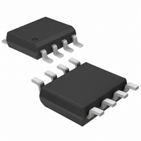
ICL7660ESA+ Maxim Integrated Products, ICL7660ESA+ Datasheet - Page 5

ICL7660ESA+
Manufacturer Part Number
ICL7660ESA+
Description
IC VOLTAGE CONVERTER 8-SOIC
Manufacturer
Maxim Integrated Products
Type
Switched Capacitor (Charge Pump), Divider, Doubler, Invertingr
Specifications of ICL7660ESA+
Internal Switch(s)
Yes
Synchronous Rectifier
No
Number Of Outputs
1
Current - Output
20mA
Frequency - Switching
10kHz
Voltage - Input
1.5 ~ 10 V
Operating Temperature
-40°C ~ 85°C
Mounting Type
Surface Mount
Package / Case
8-SOIC (3.9mm Width)
Power - Output
471mW
Function
Inverting/Step Up
Output Voltage
- 1.5 V to - 10 V or 3 V to 20 V
Output Current
20 mA
Maximum Operating Temperature
+ 85 C
Minimum Operating Temperature
- 40 C
Mounting Style
SMD/SMT
Primary Input Voltage
10V
No. Of Outputs
1
No. Of Pins
8
Operating Temperature Range
-40°C To +85°C
Dropout Voltage Vdo
500mV
Filter Terminals
SMD
Rohs Compliant
Yes
Lead Free Status / RoHS Status
Lead free / RoHS Compliant
Voltage - Output
-
Lead Free Status / Rohs Status
Lead free / RoHS Compliant
AC ELECTRICAL CHARACTERISTICS (continued)
(V
unless otherwise noted.)
Note 1: Static linearity parameters are computed from a “best-fit” straight line through the code transition points. The full-scale
Note 2: The offset control input is a self-biased voltage divider from the internal +2.5V reference voltage. The nominal open-circuit
Note 3: The clock input’s termination voltage can be operated between -2.0V and GNDI. Observe the absolute maximum ratings
Note 4: Input logic levels are measured with respect to the V
Note 5: All PECL digital outputs are loaded with 50Ω to V
Note 6: The current in the V
Note 7: Common-Mode Rejection Ratio is defined as the ratio of the change in the transfer-curve offset voltage to the change in
Note 8: Power-Supply Rejection Ratio is defined as the ratio of the change in the transfer-curve offset voltage to the change in
Note 9: Measured with the positive supplies tied to the same potential; V
Note 10: V
TIMING CHARACTERISTICS
Maximum Sample Rate
Clock Pulse Width Low
Clock Pulse Width High
Aperture Delay
Aperture Jitter
Reset Input Data Setup Time
(Note 13)
Reset Input Data Hold Time
(Note 13)
CLK to DREADY Propagation
Delay
DREADY to DATA Propagation
Delay (Note 14)
DATA Rise Time
DATA Fall Time
DREADY Rise Time
DREADY Fall Time
Primary Port Pipeline
Delay
Auxiliary Port Pipeline
Delay
CC
A = V
PARAMETER
range (FSR) is defined as 256 x slope of the line.
voltage is +1.25V. It may be driven from an external potentiometer connected between REFOUT and GNDI.
on the CLK+ and CLK- inputs.
supply voltage.
tion of the load resistance and the V
the common-mode voltage, expressed in dB.
power-supply voltage, expressed in dB.
CC
EE
I = V
varies from -5.25V to -4.75V.
CC
_______________________________________________________________________________________
D = +5.0V, V
CC
O power supply does not include the current in the digital output’s emitter followers, which is a func-
EE
SYMBOL
t
t
RDREADY
FDREADY
t
t
= -5.0V, V
RDATA
FDATA
t
f
t
t
t
t
t
PWH
MAX
PWL
t
t
PDA
t
PD1
PD2
PDP
t
AD
SU
HD
AJ
2.2GHzトラック/ホールドアンプ内蔵
TT
Figure 17
Figure 17
Figure 4
Figure 4
Figure 15
Figure 15
Figure 17
Figure 17
20% to 80%, C
20% to 80%, C
20% to 80%, C
20% to 80%, C
Figures 6, 7, 8
Figures 6, 7, 8
CC
termination voltage.
O = +3.3V, REFIN connected to REFOUT, f
CC
O - 2.0V. Measurements are made with respect to the V
L
L
L
L
CC
CONDITIONS
= 3pF
= 3pF
= 3pF
= 3pF
O power-supply voltage.
± 5V、1Gsps、8ビットADC
DIV1, DIV2 modes
DIV4 mode
DIV1, DIV2 modes
DIV4 mode
CC
A = V
CC
D = V
CC
I. V
S
= 1Gsps, f
CC
0.45
0.45
MIN
-50
1
0
0
varies from +4.75V to +5.25V.
IN
<0.5
TYP
100
150
420
360
220
180
2.2
7.5
7.5
8.5
9.5
at -1dBFS, T
MAX
350
CC
5
O power-
A
= +25°C,
UNITS
Cycles
Cycles
Clock
Clock
Gsps
ns
ns
ps
ps
ps
ps
ns
ps
ps
ps
ps
ps
5


