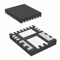
IR3870MTR1PBF International Rectifier, IR3870MTR1PBF Datasheet - Page 16

IR3870MTR1PBF
Manufacturer Part Number
IR3870MTR1PBF
Description
IC BUCK SYNC ADJ 10A PQFN56
Manufacturer
International Rectifier
Series
SupIRBuck™r
Type
Step-Down (Buck)r
Datasheet
1.IR3870MTR1PBF.pdf
(20 pages)
Specifications of IR3870MTR1PBF
Internal Switch(s)
Yes
Synchronous Rectifier
Yes
Number Of Outputs
1
Voltage - Output
0.5 ~ 12 V
Current - Output
10A
Frequency - Switching
200kHz ~ 1MHz
Voltage - Input
3 ~ 26 V
Operating Temperature
0°C ~ 125°C
Mounting Type
Surface Mount
Package / Case
17-PowerVQFN
Part Status
Active
Package
PQFN / 5 x 6
Circuit
Single Output
Iout (a)
10
Switch Freq (khz)
0 - 1000
Input Range (v)
3.0 - 26
Output Range (v)
0.5 - 12
Ocp Otp Uvlo Pre-bias Soft Start And
Constant On-Time + OVP no OTP
Lead Free Status / RoHS Status
Lead free / RoHS Compliant
Power - Output
-
Other names
IR3870MTR1PBFTR
LAYOUT RECOMMENDATION
Bypass Capacitor:
One 1uF high quality ceramic capacitor should
be placed as near VCC pin as possible. The
other end of capacitor can be connected to a
via or connected directly to GND plane. Use a
GND plane instead of thin trace to the GND pin
because this thin traces have too much higher
impedance. A 1uF is recommended for both
V5 and PVCC and repeat the layout procedure
above for those signals.
Charge Pump:
We recommend that D1, D2 and C
placed as close to the CPO and PVCC pins as
possible. If those components can not be
placed on the same layer as IR3870, a
minimum of two vias are needed for the
connection of C
connection of D2 and PVCC.
Boot Circuit:
C
PHASE pins to reduce the impedance when the
upper MOSFET turns on. D
to be close to C
current to charge C
time of lower MOSFET.
Power Stage:
Figure 19 shows the flowing current path for
the on and off periods. The on time path has
low average DC current with high AC current.
Therefore, it is recommended to place the input
ceramic capacitor, upper, and lower MOSFET
in a tight loop as shown in Figure 19.
This capacitor has 9mΩ ESR which leaves
margin for the voltage drop of the ESL during
load step up. The typical ESL for this capacitor is
around 2nH. Refer to Output Capacitor Selection
section for all ceramic capacitor solution.
BOOT
should be placed near the BOOT and
CPO
BOOT
BOOT
and CPO pin and the
because the average
is small during the on
BOOT
does not need
CPO
be
The purpose of the tight loop from the input
ceramic capacitor is to suppress the high
frequency (10MHz range) switching noise and
reduce Electromagnetic Interference (EMI). If
this path has high inductance, the circuit will
cause voltage spikes and ringing, and increase
the switching loss. The off time path has low
AC and high average DC current. Therefore, it
should be laid out with a tight loop and wide
trace at both ends of the inductor. Lowering the
loop resistance reduces the power loss. The
typical resistance value of 1-ounce copper
thickness is 0.5mΩ per square inch.
Figure 19. Current Path of Power Stage
IR3870MBF
16


