ISL8112IRZ Intersil, ISL8112IRZ Datasheet - Page 11
ISL8112IRZ
Manufacturer Part Number
ISL8112IRZ
Description
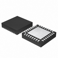
IC MAIN POWER SUPP CTRLR 32-QFN
Manufacturer
Intersil
Type
Step-Down (Buck)r
Datasheet
1.ISL8112IRZ.pdf
(27 pages)
Specifications of ISL8112IRZ
Internal Switch(s)
No
Synchronous Rectifier
Yes
Number Of Outputs
2
Voltage - Output
0.7 ~ 5.5 V
Current - Output
200mA
Voltage - Input
5.5 ~ 25 V
Operating Temperature
-40°C ~ 100°C
Mounting Type
Surface Mount
Package / Case
32-VQFN Exposed Pad, 32-HVQFN, 32-SQFN, 32-DHVQFN
Power - Output
5mW
Rohs Compliant
YES
Lead Free Status / RoHS Status
Lead free / RoHS Compliant
Frequency - Switching
-
Available stocks
Company
Part Number
Manufacturer
Quantity
Price
Company:

Part Number:
ISL8112IRZ
Manufacturer:
Intersil
Quantity:
315


Typical Application Circuits
The typical application circuits are shown in Figures 17, 18
and 19. In Figure 17, the power supply system generates
1.25V/5A and dynamic voltage/10A. Figure 18 shows
system having1.5V/5A and 1.05V/5A output. The input
supply range is 5.5V to 25V. Figure 19 shows system
having1.2V/15A and 2.5V/5A output. The input supply range
is 5.5V to 25V and 4.5V to 5.5V respectively.
Detailed Description
The ISL8112 dual-buck, BiCMOS, switch-mode power-
supply controller generates logic supply voltages for
notebook computers. The ISL8112 is designed primarily for
battery-powered applications where high efficiency and low-
quiescent supply current are critical. The ISL8112 provides a
pin-selectable switching frequency, allowing operation for
200kHz/300kHz, 400kHz/300kHz, or 400kHz/500kHz on the
SMPSs.
Light-load efficiency is enhanced by automatic Idle-Mode
operation, a variable-frequency pulse-skipping mode that
reduces transition and gate-charge losses. Each step-down,
power-switching circuit consists of two n-channel MOSFETs,
a rectifier, and an LC output filter. The output voltage is the
average AC voltage at the switching node, which is
regulated by changing the duty cycle of the MOSFET
switches. The gate-drive signal to the n-channel high-side
MOSFET must exceed the battery voltage, and is provided
by a flying-capacitor boost circuit that uses a 100nF
capacitor connected to BOOT_.
Both SMPS1 and SMPS2 PWM controllers consist of a
triple-Mode feedback network and multiplexer, a multi-input
PWM comparator, high-side and low-side gate drivers and
logic. In addition, SMPS2 can also use OUT2REF to track its
output from 0.5V to 2.50V. The ISL8112 contains fault-
protection circuits that monitor the main PWM outputs for
Typical Performance Curves
FIGURE 15. STANDBY INPUT CURRENT vs V
177.5
177.0
176.5
176.0
175.5
175.0
174.5
174.0
173.5
173.0
7
9
(EN = EN2 = 0, EN_LDO = VCC)
11
13
INPUT VOLTAGE (V)
11
15
17
19
Circuit of Figure 17 and Figure 18, no load on LDO, VSEN1, VSEN2, VREF2, and VREF1,
V
unless otherwise noted. Typical values are at T
IN
IN
= 12V, EN2 = EN1 = VCC, VBYP = 5V, PVCC = 5V, VEN_LDO = 5V, T
21
23
25
ISL8112
undervoltage and overvoltage conditions. A power-on
sequence block controls the power-up timing of the main
PWMs and monitors the outputs for undervoltage faults. The
ISL8112 includes an adjustable low drop-out linear regulator.
The bias generator blocks include the linear regulator, 3.3V
precision reference, 2V precision reference and automatic
bootstrap switch over circuit.
The synchronous-switch gate drivers are directly powered
from PVCC, while the high-side switch gate drivers are
indirectly powered from PVCC through an external capacitor
and an internal Schottky diode boost circuit.
An automatic bootstrap circuit turns off the LDO linear
regulator and powers the device from BYP if LDOREF is set
to GND or VCC. See Table 1.
FREE-RUNNING, CONSTANT ON-TIME PWM
CONTROLLER WITH INPUT FEED-FORWARD
The constant on-time PWM control architecture is a
pseudo-fixed-frequency, constant on-time, current-mode
type with voltage feed forward. The constant on-time PWM
control architecture relies on the output ripple voltage to
VOLTAGE at BYP
VOLTAGE at BYP
5V
3.3V
2 x LDOREF
FIGURE 16. SHUTDOWN INPUT CURRENT vs V
LDO VOLTAGE
26.5
26.0
25.5
25.0
24.5
24.0
23.5
23.0
22.5
22.0
7
TABLE 1. LDO OUTPUT VOLTAGE TABLE
9
(EN = EN2 = EN_LDO = 0)
A
= +25°C. (Continued)
11
LDOREF < 0.3V,
BYP > 4.63V
LDOREF > VCC - 1V,
BYP > 3V
LDOREF < 0.3V,
BYP < 4.63V
LDOREF > VCC - 1V,
BYP < 3V
0.35V <LDOREF < 2.25V
13
INPUT VOLTAGE (V)
CONDITIONS
15
17
A
= -40°C to +100°C,
19
Internal LDO is
21
Internal LDO is
disabled.
Internal LDO is
disabled.
Internal LDO is
active.
Internal LDO is
active.
active.
IN
COMMENT
August 10, 2010
23
FN6396.1
25
Related parts for ISL8112IRZ
Image
Part Number
Description
Manufacturer
Datasheet
Request
R

Part Number:
Description:
Main Power Supply Controllers
Manufacturer:
Intersil Corporation
Datasheet:
Part Number:
Description:
Intersil Corporation [CMOS Serial Controller Interface]
Manufacturer:
Intersil Corporation
Datasheet:
Part Number:
Description:
Manufacturer:
Intersil Corporation
Datasheet:
Part Number:
Description:
357-036-542-201 CARDEDGE 36POS DL .156 BLK LOPRO
Manufacturer:
Intersil Corporation
Datasheet:
Part Number:
Description:
1024-Word x 4-Bit LSI Static RAM
Manufacturer:
Intersil Corporation
Datasheet:
Part Number:
Description:
General Purpose NPN Transistor Arrays FN341.4
Manufacturer:
Intersil Corporation
Datasheet:
Part Number:
Description:
CMOS 16-Bit Microprocessor
Manufacturer:
Intersil Corporation
Datasheet:
Part Number:
Description:
Manufacturer:
Intersil Corporation
Datasheet:
Part Number:
Description:
Manufacturer:
Intersil Corporation
Datasheet:
Part Number:
Description:
Manufacturer:
Intersil Corporation
Datasheet:
Part Number:
Description:
Manufacturer:
Intersil Corporation
Datasheet:
Part Number:
Description:
CMOS 6-Bit Latch and Decoder Memory Interfaces
Manufacturer:
Intersil Corporation
Datasheet:
Part Number:
Description:
CA3046General Purpose NPN Transistor Arrays
Manufacturer:
Intersil Corporation
Datasheet:
Part Number:
Description:
Manufacturer:
Intersil Corporation
Datasheet:
Part Number:
Description:
TR909 DLC/FLC SLIC with Low Power Standby
Manufacturer:
Intersil Corporation
Datasheet: