ISL8112IRZ Intersil, ISL8112IRZ Datasheet
ISL8112IRZ
Specifications of ISL8112IRZ
Available stocks


Related parts for ISL8112IRZ

ISL8112IRZ Summary of contents
Page 1
... PART RANGE (Note) MARKING (°C) ISL8112IRZ* ISL8112 IRZ -40 to +100 32 Ld QFN *Add “-T” suffix for tape and reel. Please refer to TB347 for details on reel specifications. NOTE: These Intersil Pb-free plastic packaged products employ special Pb-free material sets, molding compounds/die attach materials, ...
Page 2
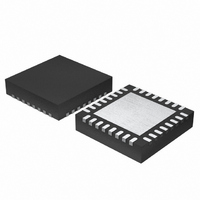
Pinout VREF1 EN_LDO VREF2 LDOREF 2 ISL8112 ISL8112 (32 LD 5X5 QFN) TOP VIEW VCC VIN 6 LDO ...
Page 3
... ISL8112 Thermal Information Thermal Resistance (Typical, Note QFN (Notes Operating Temperature Range . . . . . . . . . . . . . . . .-40°C to +100°C Junction Temperature . . . . . . . . . . . . . . . . . . . . . . . . . . . . . . +150°C Storage Temperature Range . . . . . . . . . . . . . . . . . .-65°C to +150°C Pb-Free Reflow Profile .see link below http://www.intersil.com/pbfree/Pb-FreeReflow.asp = +25°C. A CONDITIONS LDO in regulation V = LDO, VSEN1 < 4.43V 5.5V to 25V, OUT2REF > (VCC - 1V), MODE = 5V ...
Page 4
Electrical Specifications Circuit of Figure 17, and Figure 18, no load on LDO, VSEN1, VSEN2, VREF2, and VREF1, VIN = 12V, EN2 = EN1 = VCC, VBYP = 5V, PVCC = 5V, VEN_LDO = 5V, T Typical values are at ...
Page 5
Electrical Specifications Circuit of Figure 17, and Figure 18, no load on LDO, VSEN1, VSEN2, VREF2, and VREF1, VIN = 12V, EN2 = EN1 = VCC, VBYP = 5V, PVCC = 5V, VEN_LDO = 5V, T Typical values are at ...
Page 6
Electrical Specifications Circuit of Figure 17, and Figure 18, no load on LDO, VSEN1, VSEN2, VREF2, and VREF1, VIN = 12V, EN2 = EN1 = VCC, VBYP = 5V, PVCC = 5V, VEN_LDO = 5V, T Typical values are at ...
Page 7
Pin Descriptions PIN NAME VREF1 2V Reference Output. Bypass to GND with a 0.1µF (min) capacitor. VREF1 can source up to 50μA for external loads. 1 Loading VREF1 degrades FB and output accuracy according to the VREF1 load-regulation error. FS ...
Page 8
Pin Descriptions (Continued) PIN NAME LG2 SMPS2 Synchronous-Rectifier Gate-Drive Output. LG2 swings between GND and PVCC. 23 BOOT2 Boost Flying Capacitor Connection for SMPS2. Connect to an external capacitor according to the typical application 24 circuits (Figure 17 and Figure ...
Page 9
Typical Performance Curves 7 V SKIP MODE PWM MODE ULTRA SKIP MODE SKIP MODE PWM MODE IN 1.0 0.9 0.8 ...
Page 10
Typical Performance Curves 600 PWM 500 400 300 200 ULTRA-SKIP 100 SKIP 0 0.001 0.010 0.100 OUTPUT LOAD (A) FIGURE 3.3V FREQUENCY vs LOAD OUT2 450 400 350 PWM 300 250 200 150 ULTRA-SKIP 100 50 0 ...
Page 11
Typical Performance Curves 177.5 177.0 176.5 176.0 175.5 175.0 174.5 174.0 173.5 173 INPUT VOLTAGE (V) FIGURE 15. STANDBY INPUT CURRENT vs V (EN = EN2 = 0, EN_LDO = VCC) Typical Application Circuits ...
Page 12
PWM ramp signal; thus the output filter capacitor's ESR acts as a current-feedback resistor. The high-side switch on-time is determined by a one-shot whose period is inversely proportional to input voltage and directly proportional to output voltage. Another ...
Page 13
VIN: 5.5V to 25V C8 1µF C10 10µF Q3a SI4816BDY OUT1 – PCI-e C9 L1: 3.3µH 1.25V/5A 0.1µF Q3b C11 C11 330µF 9mΩ 6.3V VCC R1 7.87kΩ 5V FB1 TIED TO GND = 5V FB1 TIED TO VCC = 1.5V ...
Page 14
VIN: 5.5V to 25V C8 1µF C10 SI4816BDY 10µF Q3a OUT1 C9 L1: 3.3µH 1.5V/5A 0.1µF Q3b C11 C11 33µF 9mΩ 6.3V VCC 3.3V VCC FB1 TIED TO GND = 5V FB1 TIED TO VCC = 1.5V R3 200kΩ ON ...
Page 15
VIN: 4.5V to 5.5V VIN: 4. 1µF 1µF C10 C10 10 µ µ Q3a Q3a SI4816BDY SI4816BDY C9 C9 L2: 1.5µH L2: 1.5µH 2.5V/5A 2.5V/5A 0.1µF 0.1µF Q3b Q3b C11 C11 ...
Page 16
BOOT1 UG1 PH1 PVCC SMPS1 LG1 SYNCH. GND PWM BUCK CONTROLLER ILIM1 EN1 FB1 PGOOD1 VSEN1 VSEN1 BYP SW THRES. LDO LDO LDOREF VIN EN_LDO POWER-ON POWER-ON SEQUENCE SQUENCE EN1 CLEAR FAULT CLEAR FAULT LATCH LATCH EN2 FIGURE 20. DETAIL ...
Page 17
FS VIN VIN ILIM_ 5µA VCC PH_ VSEN_ FB DECODER FB_ Automatic Pulse-Skipping Switch Over (Idle Mode) In Idle Mode (MODE = GND), an inherent automatic switch over to PFM takes place at light loads. This switch over is affected ...
Page 18
DC output accuracy specifications refer to the trip level of the error comparator. When the inductor is in continuous conduction, the output voltage has ...
Page 19
Therefore, the exact current-limit characteristic and maximum load capability are a function of the current-limit threshold, inductor value and input and output voltage. I LOAD(MAX) I LOAD(MAX) I LOAD(MAX) ...
Page 20
Adaptive dead-time circuits monitor the LG_ and UG_ drivers and prevent either FET from turning on until the other is fully off. This algorithm allows operation without shoot- through with a wide range of MOSFETs, minimizing delays and maintaining efficiency. ...
Page 21
Discharge Mode (Soft-Stop) When a transition to standby or shutdown mode occurs, or the output is discharged to GND through an internal 25Ω switch, the reference remains active to provide an accurate threshold and to provide overvoltage protection. When the ...
Page 22
Adjustable-Output Feedback (Dual-Mode FB) Connect FB1 to GND to enable the fixed 5V or tie FB1 to VCC to set the fixed 1.5V output. Connect a resistive voltage-divider at FB1 between output and GND to adjust the respective output voltage ...
Page 23
Example 5A 12V, V LOAD(MAX 200kHz, 35% ripple current or LIR = 0.35 12V 5V – L 8.3μH ----------------------------------------------------------------- = = ⋅ ⋅ ⋅ 12V 200kHz 0.35 5A Find a ...
Page 24
⎛ ⎞ – OUT IN OUT_ ≈ ⎜ ⎟ ------------------------------------------------------------ RMS LOAD V ⎝ ⎠ IN When ⋅ IRMS has maximum 50 OUT_ ...
Page 25
For example, use an MBR0530 (500mA-rated) type for loads up to 1.5A, a 1N5817 type for loads 1N5821 type for loads up to 10A. The rectifier's rated reverse breakdown voltage must be at least ...
Page 26
... Accordingly, the reader is cautioned to verify that data sheets are current before placing orders. Information furnished by Intersil is believed to be accurate and reliable. However, no responsibility is assumed by Intersil or its subsidiaries for its use; nor for any infringements of patents or other rights of third parties which may result from its use ...
Page 27
Package Outline Drawing L32.5x5B 32 LEAD QUAD FLAT NO-LEAD PLASTIC PACKAGE Rev 3, 5/10 5.00 6 PIN 1 INDEX AREA (4X) 0.15 TOP VIEW ( 4. 80 TYP ) ( TYPICAL RECOMMENDED LAND PATTERN 27 ISL8112 A ...