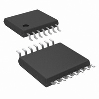
LM5010MH/NOPB National Semiconductor, LM5010MH/NOPB Datasheet - Page 17

LM5010MH/NOPB
Manufacturer Part Number
LM5010MH/NOPB
Description
IC BUCK ADJ 1A 14TSSOP
Manufacturer
National Semiconductor
Type
Step-Down (Buck)r
Datasheet
1.LM5010SDNOPB.pdf
(19 pages)
Specifications of LM5010MH/NOPB
Internal Switch(s)
Yes
Synchronous Rectifier
No
Number Of Outputs
1
Voltage - Output
2.5 ~ 70 V
Current - Output
1A
Frequency - Switching
1MHz
Voltage - Input
8 ~ 75 V
Operating Temperature
-40°C ~ 125°C
Mounting Type
Surface Mount
Package / Case
14-TSSOP Exposed Pad, 14-eTSSOP 14-HTSSOP
Primary Input Voltage
75V
No. Of Outputs
1
Output Voltage
70V
Output Current
1A
Voltage Regulator Case Style
TSSOP
No. Of Pins
14
Operating Temperature Range
-40°C To +125°C
Svhc
No SVHC (15-Dec-2010)
Rohs Compliant
Yes
Dc
1030
For Use With
LM5010 EVAL - BOARD EVALUATION LM5010
Lead Free Status / RoHS Status
Lead free / RoHS Compliant
Power - Output
-
Other names
*LM5010MH
*LM5010MH/NOPB
LM5010MH
*LM5010MH/NOPB
LM5010MH
Applications Information
where 0.11Ω is the minimum value of the internal resistance
from S
should be used for R
sary to check the average and peak current values to ensure
they do not exceed the LM5010 limits. At maximum load
current the average current through the internal sense resis-
tor is:
If I
exceeds 2.0A, R
inductor current (I
lated using the following:
where I
ceeds 3.5A , the inductor value must be increased to reduce
the ripple amplitude. This will necessitate recalculation of
I
When the circuit is in current limit, the upper peak current out
of the SW pin is
OR(min)
AVE
GND
, I
is less than 2.0A no changes are necessary. If it
OR(max)
PK-
to I
, and R
SEN
is calculated using Equation 9. If I
CL
. The next smaller standard value resistor
PK+
must be reduced. The upper peak of the
CL
CL
), at maximum load current, is calcu-
.
. With the addition of R
(Continued)
CL
it is neces-
PK+
(12)
(13)
(14)
ex-
17
The inductor L1 and diode D1 must be rated for this current.
PC BOARD LAYOUT
The LM5010 regulation, over-voltage, and current limit com-
parators are very fast, and will respond to short duration
noise pulses. Layout considerations are therefore critical for
optimum performance. The layout must be as neat and
compact as possible, and all the components must be as
close as possible to their associated pins. The current loop
formed by D1, L1, C2, and the S
as small as possible. The ground connection from C2 to C1
should be as short and direct as possible. If it is expected
that the internal dissipation of the LM5010 will produce high
junction temperatures during normal operation, good use of
the PC board’s ground plane can help considerably to dissi-
pate heat. The exposed pad on the IC package bottom can
be soldered to a ground plane, and that plane should both
extend from beneath the IC, and be connected to exposed
ground plane on the board’s other side using as many vias
as possible. The exposed pad is internally connected to the
IC substrate.
The use of wide PC board traces at the pins, where possible,
can help conduct heat away from the IC. The four No Con-
nect pins on the TSSOP package are not electrically con-
nected to any part of the IC, and may be connected to
ground plane to help dissipate heat from the package. Judi-
cious positioning of the PC board within the end product,
along with the use of any available air flow (forced or natural
convection) can help reduce the junction temperature.
GND
and I
SEN
pins should be
www.national.com


