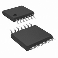
LM5010MH/NOPB National Semiconductor, LM5010MH/NOPB Datasheet

LM5010MH/NOPB
Specifications of LM5010MH/NOPB
*LM5010MH/NOPB
LM5010MH
Related parts for LM5010MH/NOPB
LM5010MH/NOPB Summary of contents
Page 1
... The valley current limit detection is set at 1.25A. Additional features include: V lockout, thermal shutdown, gate drive under-voltage lockout, and maximum duty cycle limiter. © 2005 National Semiconductor Corporation Features n Input Voltage Range 75V n Valley Current Limit At 1.25A n Switching Frequency Can Exceed 1 MHz ...
Page 2
Connection Diagrams Ordering Information Order Number Package Type LM5010SD LLP-10 (4x4) LM5010SDX LLP-10 (4x4) LM5010MH TSSOP-14EP LM5010MHX TSSOP-14EP www.national.com 20119902 NSC Package Drawing SDC10A SDC10A MXA14A MXA14A 2 20119903 Supplied As 1000 Units on Tape and Reel 4500 Units on ...
Page 3
Pin Description PIN NUMBER LLP-10 TSSOP-14 NAME BST SEN GND 5 6 RTN / ...
Page 4
... Absolute Maximum Ratings If Military/Aerospace specified devices are required, please contact the National Semiconductor Sales Office/ Distributors for availability and specifications GND IN BST to GND SW to GND (Steady State) BST BST GND RTN GND SS to RTN Electrical Charateristics Specifications with standard typeface are for T Temperature range ...
Page 5
... Device thermal limitations limit external loading. CC Note 4: For detailed information on soldering plastic TSSOP and LLP packages refer to the Packaging Data Book available from National Semiconductor Corporation. Note 5: Typical specifications represent the most likely parametric norm at 25˚C operation. ...
Page 6
Typical Application Circuit and Block Diagram (pin numbers are for the LLP-10 package) www.national.com FIGURE 1. 6 20119944 ...
Page 7
Typical Performance Characteristics FIGURE FIGURE 20119904 FIGURE 20119905 CC 7 20119906 vs Externally Applied 20119907 FIGURE 5. On-Time vs V and ...
Page 8
Typical Performance Characteristics (Continued) FIGURE 6. Voltage at R www.national.com 20119908 /SD Pin ON 8 20119910 FIGURE ...
Page 9
Typical Performance Characteristics Functional Description The LM5010 Step Down Switching Regulator features all the functions needed to implement a low cost, efficient buck bias power converter capable of supplying in excess the load. This high voltage regulator ...
Page 10
Hysteretic Control Circuit Overview (Continued) Typically when the load current increases suddenly, the off- times are temporarily at the minimum of 265 ns. Once regu- lation is established, the off-time resumes its normal value. The output voltage is set by ...
Page 11
Start-up Regulator (V CC Regulation Comparator The feedback voltage compared to the voltage at the ± Softstart pin (2.5V, 2%). In normal operation (the output voltage is regulated) an on-time period is initiated when the voltage at ...
Page 12
Current Limit Current limit detection occurs during the off-time by monitor- ing the recirculating current through the free-wheeling diode (D1). The detection threshold is 1.25A, Figure 1, when the buck switch is off the inductor current flows through the load, ...
Page 13
Thermal Shutdown (Continued) heating. When the junction temperature reduces below 155˚C (typical hysteresis = 20˚C), the Softstart pin is re- leased and normal operation resumes. Applications Information EXTERNAL COMPONENTS The procedure for calculating the external components is illustrated with a ...
Page 14
Applications Information The minimum ESR for C2 is then equal to: If the capacitor used for C2 does not have sufficient ESR added in series as shown in Figure 1. C2 should generally be no smaller than 3.3 ...
Page 15
Applications Information Item Description C1 Ceramic Capacitor C2 Ceramic Capacitor C3 Ceramic Capacitor C4, C6 Ceramic Capacitor C5 Ceramic Capacitor D1 Ultra fast diode L1 Inductor R1 Resistor R2 Resistor R3 Resistor R Resistor ON U1 Switching regulator (Continued) FIGURE ...
Page 16
Applications Information FIGURE 15. Efficiency vs V Circuit of Figure 14 FIGURE 16. Efficiency vs Load Current and V Circuit of Figure 14 www.national.com (Continued) FIGURE 17. Output Voltage Ripple vs V 20119934 IN FIGURE 18. Frequency vs V 20119935 ...
Page 17
Applications Information where 0.11Ω is the minimum value of the internal resistance from The next smaller standard value resistor GND SEN should be used for R . With the addition sary to check ...
Page 18
Physical Dimensions www.national.com inches (millimeters) unless otherwise noted 14-Lead TSSOP Package NS Package Number MXA14A 10-Lead LLP Package NS Package Number SDC10A 18 ...
Page 19
... BANNED SUBSTANCE COMPLIANCE National Semiconductor manufactures products and uses packing materials that meet the provisions of the Customer Products Stewardship Specification (CSP-9-111C2) and the Banned Substances and Materials of Interest Specification (CSP-9-111S2) and contain no ‘‘Banned Substances’’ as defined in CSP-9-111S2. ...


