LM5574MT/NOPB National Semiconductor, LM5574MT/NOPB Datasheet - Page 8
LM5574MT/NOPB
Manufacturer Part Number
LM5574MT/NOPB
Description
IC BUCK SYNC ADJ .5A 16TSSOP
Manufacturer
National Semiconductor
Series
PowerWise®, SIMPLE SWITCHER®r
Type
Step-Down (Buck)r
Specifications of LM5574MT/NOPB
Internal Switch(s)
Yes
Synchronous Rectifier
No
Number Of Outputs
1
Voltage - Output
1.23 ~ 70 V
Current - Output
500mA
Frequency - Switching
200kHz, 485kHz
Voltage - Input
6 ~ 75 V
Operating Temperature
-40°C ~ 125°C
Mounting Type
Surface Mount
Package / Case
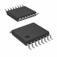
16-TSSOP
Power - Output
700mW
Current, Input Bias
3.7 mA
Current, Input Offset
50 μA
Current, Output
0.5 A
Frequency, Oscillator
200/485 kHz
Package Type
TSSOP
Regulator Type
Buck (Step-Down), Switching
Resistance, Thermal, Junction To Case
30 °C/W
Temperature, Operating, Range
-40 to +125 °C
Voltage, Input
6 to 75 V
Voltage, Offset
0.7 V (COMP to PWM Comparator)
Voltage, Output
7.15 V
Dc To Dc Converter Type
Step Down
Pin Count
16
Input Voltage
75V
Output Voltage
1.225 to 70V
Switching Freq
50 TO 500KHz
Output Current
500mA
Efficiency
85%
Output Type
Adjustable
Switching Regulator
Yes
Mounting
Surface Mount
Input Voltage (min)
6V
Operating Temp Range
-40C to 125C
Operating Temperature Classification
Automotive
For Use With
LM5574BLDT - WEBENCH BUILD IT BOARD LM5574LM5574EVAL - BOARD EVALUATION FOR LM5574
Lead Free Status / RoHS Status
Lead free / RoHS Compliant
Other names
*LM5574MT
*LM5574MT/NOPB
LM5574MT
*LM5574MT/NOPB
LM5574MT
Available stocks
Company
Part Number
Manufacturer
Quantity
Price
Company:

Part Number:
LM5574MT/NOPB
Manufacturer:
NS
Quantity:
8 500
Part Number:
LM5574MT/NOPB
Manufacturer:
TI/德州仪器
Quantity:
20 000


www.national.com
Detailed Operating Description
The LM5574 switching regulator features all of the functions
necessary to implement an efficient high voltage buck regu-
lator using a minimum of external components. This easy to
use regulator integrates a 75V N-Channel buck switch with
an output current capability of 0.5 Amps. The regulator control
method is based on current mode control utilizing an emulat-
ed current ramp. Peak current mode control provides inherent
line voltage feed-forward, cycle-by-cycle current limiting, and
ease of loop compensation. The use of an emulated control
ramp reduces noise sensitivity of the pulse-width modulation
circuit, allowing reliable processing of very small duty cycles
necessary in high input voltage applications. The operating
frequency is user programmable from 50kHz to 500kHz. An
oscillator synchronization pin allows multiple LM5574 regula-
tors to self synchronize or be synchronized to an external
clock. The output voltage can be set as low as 1.225V. Fault
protection features include, current limiting, thermal shutdown
and remote shutdown capability. The device is available in the
TSSOP-16 package.
The functional block diagram and typical application of the
LM5574 are shown in Figure 1. The LM5574 can be applied
in numerous applications to efficiently step-down a high, un-
regulated input voltage. The device is well suited for telecom,
industrial and automotive power bus voltage ranges.
High Voltage Start-Up Regulator
The LM5574 contains a dual-mode internal high voltage start-
up regulator that provides the Vcc bias supply for the PWM
controller and boot-strap MOSFET gate driver. The input pin
FIGURE 2. Vin and Vcc Sequencing
8
(VIN) can be connected directly to the input voltage, as high
as 75 Volts. For input voltages below 9V, a low dropout switch
connects Vcc directly to Vin. In this supply range, Vcc is ap-
proximately equal to Vin. For Vin voltage greater than 9V, the
low dropout switch is disabled and the Vcc regulator is en-
abled to maintain Vcc at approximately 7V. The wide operat-
ing range of 6V to 75V is achieved through the use of this dual
mode regulator.
The output of the Vcc regulator is current limited to 25mA.
Upon power up, the regulator sources current into the capac-
itor connected to the VCC pin. When the voltage at the VCC
pin exceeds the Vcc UVLO threshold of 5.35V and the SD pin
is greater than 1.225V, the output switch is enabled and a soft-
start sequence begins. The output switch remains enabled
until Vcc falls below 5.0V or the SD pin falls below 1.125V.
An auxiliary supply voltage can be applied to the Vcc pin to
reduce the IC power dissipation. If the auxiliary voltage is
greater than 7.3V, the internal regulator will essentially
shut off, reducing the IC power dissipation. The Vcc regulator
series pass transistor includes a diode between Vcc and Vin
that should not be forward biased in normal operation. There-
fore the auxiliary Vcc voltage should never exceed the Vin
voltage.
In high voltage applications extra care should be taken to en-
sure the VIN pin does not exceed the absolute maximum
voltage rating of 76V. During line or load transients, voltage
ringing on the Vin line that exceeds the Absolute Maximum
Ratings can damage the IC. Both careful PC board layout and
the use of quality bypass capacitors located close to the VIN
and GND pins are essential.
20212004
Related parts for LM5574MT/NOPB
Image
Part Number
Description
Manufacturer
Datasheet
Request
R

Part Number:
Description:
IC,SMPS CONTROLLER,CURRENT-MODE,TSSOP,16PIN,PLASTIC
Manufacturer:
National Semiconductor
Part Number:
Description:
National Semiconductor [8-Bit D/A Converter]
Manufacturer:
National Semiconductor
Datasheet:
Part Number:
Description:
National Semiconductor [Media Coprocessor]
Manufacturer:
National Semiconductor
Datasheet:
Part Number:
Description:
Digitally Controlled Tone and Volume Circuit with Stereo Audio Power Amplifier, Microphone Preamp Stage and National 3D Sound
Manufacturer:
National Semiconductor
Datasheet:
Part Number:
Description:
Digitally Controlled Tone and Volume Circuit with Stereo Audio Power Amplifier, Microphone Preamp Stage and National 3D Sound
Manufacturer:
National Semiconductor
Datasheet:
Part Number:
Description:
AC97 Rev 2 Codec with Sample Rate Conversion and National 3D Sound
Manufacturer:
National Semiconductor
Part Number:
Description:
Manufacturer:
National Semiconductor
Datasheet:
Part Number:
Description:
Manufacturer:
National Semiconductor
Datasheet:
Part Number:
Description:
General Purpose, Low Voltage, Low Power, Rail-to-Rail Output Operational Amplifiers
Manufacturer:
National Semiconductor
Datasheet:
Part Number:
Description:
8-bit 20 MSPS flash A/D converter.
Manufacturer:
National Semiconductor
Datasheet:
Part Number:
Description:
Low Noise Quad Operational Amplifier
Manufacturer:
National Semiconductor
Datasheet:
Part Number:
Description:
Quad Differential Line Receivers
Manufacturer:
National Semiconductor
Datasheet:
Part Number:
Description:
Quad High Speed Trapezoidal? Bus Transceiver
Manufacturer:
National Semiconductor
Datasheet:
Part Number:
Description:
Dual Line Receiver
Manufacturer:
National Semiconductor
Datasheet: