LM5574MT/NOPB National Semiconductor, LM5574MT/NOPB Datasheet - Page 3
LM5574MT/NOPB
Manufacturer Part Number
LM5574MT/NOPB
Description
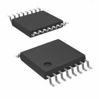
IC BUCK SYNC ADJ .5A 16TSSOP
Manufacturer
National Semiconductor
Series
PowerWise®, SIMPLE SWITCHER®r
Type
Step-Down (Buck)r
Specifications of LM5574MT/NOPB
Internal Switch(s)
Yes
Synchronous Rectifier
No
Number Of Outputs
1
Voltage - Output
1.23 ~ 70 V
Current - Output
500mA
Frequency - Switching
200kHz, 485kHz
Voltage - Input
6 ~ 75 V
Operating Temperature
-40°C ~ 125°C
Mounting Type
Surface Mount
Package / Case
16-TSSOP
Power - Output
700mW
Current, Input Bias
3.7 mA
Current, Input Offset
50 μA
Current, Output
0.5 A
Frequency, Oscillator
200/485 kHz
Package Type
TSSOP
Regulator Type
Buck (Step-Down), Switching
Resistance, Thermal, Junction To Case
30 °C/W
Temperature, Operating, Range
-40 to +125 °C
Voltage, Input
6 to 75 V
Voltage, Offset
0.7 V (COMP to PWM Comparator)
Voltage, Output
7.15 V
Dc To Dc Converter Type
Step Down
Pin Count
16
Input Voltage
75V
Output Voltage
1.225 to 70V
Switching Freq
50 TO 500KHz
Output Current
500mA
Efficiency
85%
Output Type
Adjustable
Switching Regulator
Yes
Mounting
Surface Mount
Input Voltage (min)
6V
Operating Temp Range
-40C to 125C
Operating Temperature Classification
Automotive
For Use With
LM5574BLDT - WEBENCH BUILD IT BOARD LM5574LM5574EVAL - BOARD EVALUATION FOR LM5574
Lead Free Status / RoHS Status
Lead free / RoHS Compliant
Other names
*LM5574MT
*LM5574MT/NOPB
LM5574MT
*LM5574MT/NOPB
LM5574MT
Available stocks
Company
Part Number
Manufacturer
Quantity
Price
Company:

Part Number:
LM5574MT/NOPB
Manufacturer:
NS
Quantity:
8 500
Part Number:
LM5574MT/NOPB
Manufacturer:
TI/德州仪器
Quantity:
20 000


Pin Descriptions
Pin(s)
10
11
12
13
14
15
16
1
2
3
4
5
6
7
8
9
COMP
RAMP
AGND
PGND
Name
SYNC
VCC
OUT
PRE
BST
SW
SD
Vin
RT
SS
FB
IS
Output of the bias regulator
Shutdown or UVLO input
Input supply voltage
Oscillator synchronization input or output The internal oscillator can be synchronized to an external
Output of the internal error amplifier
Feedback signal from the regulated
output
Internal oscillator frequency set input
Ramp control signal
Analog ground
Soft-start
Output voltage connection
Power ground
Current sense
Switching node
Pre-charge assist for the bootstrap
capacitor
Boost input for bootstrap capacitor
Description
3
Vcc tracks Vin up to 9V. Beyond 9V, Vcc is regulated to 7
Volts. A 0.1uF to 1uF ceramic decoupling capacitor is
required. An external voltage (7.5V – 14V) can be applied
to this pin to reduce internal power dissipation.
If the SD pin voltage is below 0.7V the regulator will be in a
low power state. If the SD pin voltage is between 0.7V and
1.225V the regulator will be in standby mode. If the SD pin
voltage is above 1.225V the regulator will be operational. An
external voltage divider can be used to set a line
undervoltage shutdown threshold. If the SD pin is left open
circuit, a 5µA pull-up current source configures the regulator
fully operational.
Nominal operating range: 6V to 75V
clock with an external pull-down device. Multiple LM5574
devices can be synchronized together by connection of their
SYNC pins.
The loop compensation network should be connected
between this pin and the FB pin.
This pin is connected to the inverting input of the internal
error amplifier. The regulation threshold is 1.225V.
The internal oscillator is set with a single resistor, connected
between this pin and the AGND pin.
An external capacitor connected between this pin and the
AGND pin sets the ramp slope used for current mode
control. Recommended capacitor range 50pF to 2000pF.
Internal reference for the regulator control functions
An external capacitor and an internal 10µA current source
set the time constant for the rise of the error amp reference.
The SS pin is held low during standby, Vcc UVLO and
thermal shutdown.
Connect directly to the regulated output voltage.
Low side reference for the PRE switch and the IS sense
resistor.
Current measurement connection for the re-circulating
diode. An internal sense resistor and a sample/hold circuit
sense the diode current near the conclusion of the off-time.
This current measurement provides the DC level of the
emulated current ramp.
The source terminal of the internal buck switch. The SW pin
should be connected to the external Schottky diode and to
the buck inductor.
This open drain output can be connected to SW pin to aid
charging the bootstrap capacitor during very light load
conditions or in applications where the output may be pre-
charged before the LM5574 is enabled. An internal pre-
charge MOSFET is turned on for 250ns each cycle just prior
to the on-time interval of the buck switch.
An external capacitor is required between the BST and the
SW pins. A 0.022µF ceramic capacitor is recommended.
The capacitor is charged from Vcc via an internal diode
during the off-time of the buck switch.
Application Information
www.national.com
Related parts for LM5574MT/NOPB
Image
Part Number
Description
Manufacturer
Datasheet
Request
R

Part Number:
Description:
IC,SMPS CONTROLLER,CURRENT-MODE,TSSOP,16PIN,PLASTIC
Manufacturer:
National Semiconductor
Part Number:
Description:
National Semiconductor [8-Bit D/A Converter]
Manufacturer:
National Semiconductor
Datasheet:
Part Number:
Description:
National Semiconductor [Media Coprocessor]
Manufacturer:
National Semiconductor
Datasheet:
Part Number:
Description:
Digitally Controlled Tone and Volume Circuit with Stereo Audio Power Amplifier, Microphone Preamp Stage and National 3D Sound
Manufacturer:
National Semiconductor
Datasheet:
Part Number:
Description:
Digitally Controlled Tone and Volume Circuit with Stereo Audio Power Amplifier, Microphone Preamp Stage and National 3D Sound
Manufacturer:
National Semiconductor
Datasheet:
Part Number:
Description:
AC97 Rev 2 Codec with Sample Rate Conversion and National 3D Sound
Manufacturer:
National Semiconductor
Part Number:
Description:
Manufacturer:
National Semiconductor
Datasheet:
Part Number:
Description:
Manufacturer:
National Semiconductor
Datasheet:
Part Number:
Description:
General Purpose, Low Voltage, Low Power, Rail-to-Rail Output Operational Amplifiers
Manufacturer:
National Semiconductor
Datasheet:
Part Number:
Description:
8-bit 20 MSPS flash A/D converter.
Manufacturer:
National Semiconductor
Datasheet:
Part Number:
Description:
Low Noise Quad Operational Amplifier
Manufacturer:
National Semiconductor
Datasheet:
Part Number:
Description:
Quad Differential Line Receivers
Manufacturer:
National Semiconductor
Datasheet:
Part Number:
Description:
Quad High Speed Trapezoidal? Bus Transceiver
Manufacturer:
National Semiconductor
Datasheet:
Part Number:
Description:
Dual Line Receiver
Manufacturer:
National Semiconductor
Datasheet: