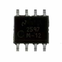
LM2597M-12/NOPB National Semiconductor, LM2597M-12/NOPB Datasheet - Page 12

LM2597M-12/NOPB
Manufacturer Part Number
LM2597M-12/NOPB
Description
IC REG SIMPLE SWITCHER 8-SOIC
Manufacturer
National Semiconductor
Series
SIMPLE SWITCHER®r
Type
Step-Down (Buck)r
Datasheet
1.LM2597M-3.3NOPB.pdf
(34 pages)
Specifications of LM2597M-12/NOPB
Internal Switch(s)
Yes
Synchronous Rectifier
No
Number Of Outputs
1
Voltage - Output
12V
Current - Output
500mA
Frequency - Switching
150kHz
Voltage - Input
4.5 ~ 40 V
Operating Temperature
-40°C ~ 125°C
Mounting Type
Surface Mount
Package / Case
8-SOIC (3.9mm Width)
Supply Voltage Range
4.5V To 40V
Termination Type
SMD
Driver Case Style
NSOIC
No. Of Pins
8
Output Voltage Min
1.23V
Voltage Regulator Type
Buck Switching
Rohs Compliant
Yes
Filter Terminals
SMD
Input Voltage Primary Max
40V
Leaded Process Compatible
Yes
No. Of Outputs
1
Lead Free Status / RoHS Status
Lead free / RoHS Compliant
Power - Output
-
Other names
*LM2597M-12
*LM2597M-12/NOPB
LM2597M-12
*LM2597M-12/NOPB
LM2597M-12
www.national.com
Given:
V
V
I
F = Switching Frequency (Fixed at a nominal 150 kHz).
1. Programming Output Voltage (Selecting R
shown in Figure 12 )
Use the following formula to select the appropriate resistor
values.
Select a value for R
resistor values minimize noise pickup in the sensitive feed-
back pin. (For the lowest temperature coefficient and the best
stability with time, use 1% metal film resistors.)
2. Inductor Selection (L1)
A. Calculate the inductor Volt microsecond constant E • T
(V • µs), from the following formula:
where V
and V
B. Use the E • T value from the previous formula and match
it with the E • T number on the vertical axis of the Inductor
Value Selection Guide shown in Figure 6 .
C. on the horizontal axis, select the maximum load current.
D. Identify the inductance region intersected by the E • T
value and the Maximum Load Current value. Each region is
identified by an inductance value and an inductor code (LXX).
E. Select an appropriate inductor from the four manufacturer’s
part numbers listed in Figure 7 .
LM2597/LM2597HV Series Buck Regulator Design Procedure (Adjustable
Output)
LOAD
OUT
IN
(max) = Maximum Input Voltage
PROCEDURE (Adjustable Output Voltage Version)
(max) = Maximum Load Current
D
= Regulated Output Voltage
= diode forward voltage drop = 0.5V
SAT
= internal switch saturation voltage = 0.9V
1
between 240
and 1.5 k . The lower
1
and R
2
, as
12
Given:
V
V
I
F = Switching Frequency (Fixed at a nominal 150 kHz).
1. Programming Output Voltage (Selecting R
Select R
R
R
2. Inductor Selection (L1)
A. Calculate the inductor Volt • microsecond constant (E • T),
B. E • T = 35.2 (V • µs)
C. I
D. From the inductor value selection guide shown in Figure 6 ,
inductor part number from the list of manufacturers part num-
bers.
shown in Figure 12 )
the inductance region intersected by the 35 (V • µs) horizontal
line and the 0.5A vertical line is 150 µH, and the inductor code
is L19.
E. From the table in Figure 7 , locate line L19, and select an
LOAD
OUT
IN
2
2
(max) = 28V
= 1k (16.26 − 1) = 15.26k, closest 1% value is 15.4 k .
= 15.4 k .
LOAD
EXAMPLE (Adjustable Output Voltage Version)
(max) = 0.5A
= 20V
(max) = 0.5A
1
to be 1 k , 1%. Solve for R
2
.
1
and R
2
, as


