LM78S40CN/NOPB National Semiconductor, LM78S40CN/NOPB Datasheet - Page 3
LM78S40CN/NOPB
Manufacturer Part Number
LM78S40CN/NOPB
Description
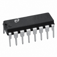
IC MULTI CONFIG ADJ 1.5A 16DIP
Manufacturer
National Semiconductor
Type
Step-Down (Buck), Step-Up (Boost), Invertingr
Specifications of LM78S40CN/NOPB
Internal Switch(s)
Yes
Synchronous Rectifier
No
Number Of Outputs
1
Voltage - Output
1.25 ~ 40 V
Current - Output
1.5A
Frequency - Switching
100kHz
Voltage - Input
2.5 ~ 40 V
Operating Temperature
0°C ~ 70°C
Mounting Type
Through Hole
Package / Case
16-DIP (0.300", 7.62mm)
Power - Output
1.04W
Common Mode Rejection Ratio
76
Current, Input Bias
35 nA (Comparator), 30 nA (Operational Amplifier)
Current, Input Offset
5 nA
Current, Output
1.5 A
Current, Supply
2.3 mA
Package Type
DIP-16
Power Dissipation
1.04 W
Regulation, Line
0.04 mV/V
Regulation, Load
0.2 mV/mA
Regulator Type
Switching, Step-Up, Step-Down
Temperature, Operating, Range
-40 to +125 °C
Voltage, Input
2.5 to 40 V
Voltage, Offset
1.5 mV (Comparator), 4 mV (Operational Amplifier)
Voltage, Output
1.25 to 40 V
Voltage, Supply, Rejection Ratio
76 dB
Lead Free Status / RoHS Status
Lead free / RoHS Compliant
Other names
*LM78S40CN
*LM78S40CN/NOPB
78S40
LM78S40CN
*LM78S40CN/NOPB
78S40
LM78S40CN


4
OUTPUT SWITCH SECTION
h
I
POWER DIODE
V
I
COMPARATOR
V
I
I
V
PSRR
OPERATIONAL AMPLIFIER
V
I
I
A
A
V
CMR
PSRR
I
I
SR
V
V
Symbol
L
DR
IB
IO
IB
IO
O
O
FE
T
FD
IO
CM
IO
VS
VS
CM
OL
OH
LM78S40
Electrical Characteristics
Note 1: Absolute Maximum Ratings indicate limits beyond which damage to the device may occur. Electrical specifications do not apply when ordering the device
beyond its rated operating conditions.
Note 2: T
Note 3: Ratings apply to ambient temperature at 25˚C. Above this temperature, derate the 16L-Ceramic DIP at 10 mW/˚C, and the 16L-Molded DIP at 8.3 mW/˚C.
Note 4: For supply voltages less than 30V, the absolute maximum voltage is equal to the supply voltage.
Note 5: A military RETS specification is available on request. At the time of printing, the LM78S40 RETS specification complied with the Min and Max limits in this
table. The LM78S40J may also be procured as a Standard Military Drawing.
+
−
A
+
−
= Operating temperature range, V
J Max
Output Transistor Current
Gain
Output Leakage Current
Forward Voltage Drop
Diode Leakage Current
Input Offset Voltage
Input Bias Current
Input Offset Current
Common Mode Voltage
Range
Power Supply Rejection
Ratio
Input Offset Voltage
Input Bias Current
Input Offset Current
Voltage Gain
Voltage Gain
Common Mode Voltage
Range
Common Mode Rejection
Power Supply Rejection
Ratio
Output Source Current
Output Sink Current
Slew Rate
Output Voltage LOW
Output Voltage High
= 150˚C for the Molded DIP, and 175˚C for the Ceramic DIP.
Parameter
+
−
IN
= 5.0V, V
V
R
R
V
V
V
I
V
I
V
V
V
V
T
V
V
V
V
T
T
T
T
I
I
C
D
L
L
A
A
A
A
A
O
D
CM
CM
CM
IN
CM
CM
CM
O
O
CM
+
L
L
(Note 5) (Continued)
= −5.0 mA, T
= 50 mA, T
= 1.0A, V
= 1.0A
(Op Amp) = 3.0V to 40V, T
= 25˚C
= 2.0 k
= 2.0 k
= 25˚C
= 25˚C
= 25˚C
= 25˚C
= 40V, T
= 40V, T
= 1.0V to 2.5V, T
= 1.0V to 2.5V, T
= 3.0V to 40V, T
= V
= V
= V
= 2.5V
= 2.5V
= 2.5V
= 0V to 3.0V, T
+
REF
REF
REF
(Op Amp) = 5.0V, unless otherwise specified.
CE
A
A
to GND;
to V
A
= 25˚C
= 25˚C
= 5.0V, T
A
= 25˚C
+
Conditions
= 25˚C
(Op Amp)
A
A
A
A
= 25˚C
= 25˚C
= 25˚C
= 25˚C
A
= 25˚C
A
= 25˚C
V + (Op
Amp) −
Min
70
25
76
76
75
10
3V
25
0
0
1.25
Typ
250
250
100
100
150
1.5
5.0
4.0
5.0
0.6
70
10
10
35
96
30
35
V
V
CC
Max
200
200
1.5
IN
1.0
15
75
15
75
–2
− 2
Units
V/mV
V/mV
V/µs
mV
mV
mA
mA
nA
nA
nA
nA
dB
nA
dB
dB
nA
V
V
V
V
V
Related parts for LM78S40CN/NOPB
Image
Part Number
Description
Manufacturer
Datasheet
Request
R

Part Number:
Description:
IC, SWITCHING REGULATOR SUBSYSTEM, 16-DIP
Manufacturer:
National Semiconductor
Datasheet:

Part Number:
Description:
Universal Switching Regulator Subsystem
Manufacturer:
National Semiconductor Corporation
Datasheet:
Part Number:
Description:
Universal Switching Regulator Subsystem
Manufacturer:
NSC [National Semiconductor]
Datasheet:
Part Number:
Description:
National Semiconductor [8-Bit D/A Converter]
Manufacturer:
National Semiconductor
Datasheet:
Part Number:
Description:
National Semiconductor [Media Coprocessor]
Manufacturer:
National Semiconductor
Datasheet:
Part Number:
Description:
Digitally Controlled Tone and Volume Circuit with Stereo Audio Power Amplifier, Microphone Preamp Stage and National 3D Sound
Manufacturer:
National Semiconductor
Datasheet:
Part Number:
Description:
Digitally Controlled Tone and Volume Circuit with Stereo Audio Power Amplifier, Microphone Preamp Stage and National 3D Sound
Manufacturer:
National Semiconductor
Datasheet:
Part Number:
Description:
AC97 Rev 2 Codec with Sample Rate Conversion and National 3D Sound
Manufacturer:
National Semiconductor
Part Number:
Description:
Manufacturer:
National Semiconductor
Datasheet:
Part Number:
Description:
Manufacturer:
National Semiconductor
Datasheet:
Part Number:
Description:
General Purpose, Low Voltage, Low Power, Rail-to-Rail Output Operational Amplifiers
Manufacturer:
National Semiconductor
Datasheet:
Part Number:
Description:
8-bit 20 MSPS flash A/D converter.
Manufacturer:
National Semiconductor
Datasheet:
Part Number:
Description:
Low Noise Quad Operational Amplifier
Manufacturer:
National Semiconductor
Datasheet:
Part Number:
Description:
Quad Differential Line Receivers
Manufacturer:
National Semiconductor
Datasheet: