L4970A STMicroelectronics, L4970A Datasheet - Page 3
L4970A
Manufacturer Part Number
L4970A
Description
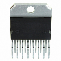
IC BUCK SYNC ADJ 10A MULTIWATT15
Manufacturer
STMicroelectronics
Type
Step-Down (Buck)r
Specifications of L4970A
Internal Switch(s)
Yes
Synchronous Rectifier
No
Number Of Outputs
1
Voltage - Output
5.1 ~ 40 V
Current - Output
10A
Frequency - Switching
200kHz
Voltage - Input
15 ~ 50 V
Operating Temperature
0°C ~ 125°C
Mounting Type
Through Hole
Package / Case
Multiwatt-15 (Vertical, Bent and Staggered Leads)
Power - Output
30W
Output Voltage
40 V
Output Current
10 A
Input Voltage
15 V to 50 V
Switching Frequency
180 KHz to 220 KHz
Operating Temperature Range
- 40 C to + 150 C
Mounting Style
Through Hole
Duty Cycle (max)
90 %
Current, Input Bias
0.4 μA
Current, Output
10 A
Current, Supply
13 mA
Frequency, Oscillator
200 kHz
Package Type
Multiwatt
Power Dissipation
30 W
Regulation, Line
10 mV
Regulation, Load
20 mV
Regulator Type
Switching
Resistance, Thermal, Junction To Case
1 °C/W
Temperature, Operating, Range
-40 to +150 °C
Voltage, Dropout
1.1 V
Voltage, Gain
60 dB
Voltage, Input
50 V
Voltage, Offset
2 mV
Voltage, Output
5.1 V
Voltage, Output, High
5.5 V
Voltage, Output, Low
0.9 V
Voltage, Supply, Rejection Ratio
80 dB
No. Of Outputs
1
Power Dissipation Pd
30W
No. Of Pins
15
Filter Terminals
Through Hole
Rohs Compliant
Yes
Lead Free Status / RoHS Status
Lead free / RoHS Compliant
Other names
497-1410-5
Available stocks
Company
Part Number
Manufacturer
Quantity
Price
Company:

Part Number:
L4970A
Manufacturer:
STMicroel
Quantity:
620
Part Number:
L4970A
Manufacturer:
ST
Quantity:
20 000
Company:
Part Number:
L4970A L297 L298 L6203 L6219 L6225 L6205
Manufacturer:
ST
0


PIN FUNCTIONS
CIRCUIT OPERATION (refer to the block dia-
gram)
The L4970A is a 10A monolithic stepdown switching
regulator working in continuous mode realized in the
new BCD Technology. This technology allows the in-
tegration of isolated vertical DMOS power transistors
plus mixed CMOS/Bipolar transistors.
The device can deliver 10A at an output voltage
adjustable from 5.1V to 40V, and contains diag-
nostic and control functions that make it particu-
larly suitable for microprocessor based systems.
BLOCK DIAGRAM
The block diagram shows the DMOS power tran-
sistor and the PWM control loop. Integrated func-
tions include a reference voltage trimmed to 5.1V
with feedforward control, pulse by pulse current
limit, thermal shutdown and finally the reset and
power fail circuit. The reset and power fail circuit
provides an output signal for a microprocessor in-
dicating the status of the system.
2%, soft start, undervoltage lockout, oscillator
N
10
11
12
13
14
15
1
2
3
4
5
6
7
8
9
o
OSCILLATOR
OSCILLATOR
RESET INPUT
RESET OUT
RESET DELAY
BOOTSTRAP
OUTPUT
GROUND
SUPPLY VOLTAGE
FREQUENCY
COMPENSATION
FEEDBACK INPUT
SOFT START
SYNC INPUT
V
V
ref
start
Name
R
current of C
C
switching frequency.
Input of Power Fail Circuit. The threshold is 5.1V. It may be connected via a
divider to the input for power fail function. It must be connected to the pin 14 an
external 30K resistor when power fail signal not required.
Open Collector Reset/power Fail Signal Output. This output is high when the
supply and the output voltages are safe.
A C
reset signal delay time.
A C
drive properly the internal D-MOS transistor.
Regulator Output.
Common Ground Terminal
Unregulated Input Voltage.
A series RC network connected between this terminal and ground determines
the regulation loop gain characteristics.
The Feedback Terminal of the Regulation Loop. The output is connected
directly to this terminal for 5.1V operation; It is connected via a divider for higher
voltages.
Soft Start Time Constant. A capacitor is connected between thi sterminal and
ground to define the soft start time constant.
Multiple L4970A are synchronized by connecting pin 13 inputs together or via
an external syncr. pulse.
5.1V V
Internal Start-up Circuit to Drive the Power Stage.
osc
osc
d
boot
. External resistor connected to ground determines the constant charging
. External capacitor connected to ground determines (with R
capacitor connected between this terminal and ground determines the
ref
capacitor connected between this terminal and the output allows to
Device Reference Voltage.
osc
.
Device turn on is around 11V with a typical 1V
hysteresis, this threshold provides a correct volt-
age for the driving stage of the DMOS gate and
the hysteresis prevents instabilities.
An external bootstrap capacitor charged to 12V
by an internal voltage reference is needed to pro-
vide correct gate drive to the power DMOS. The
driving circuit is able to source and sink peak cur-
rents of around 0.5A to the gate of the DMOS
transistor. A typical switching time of the current
in the DMOS transistor is 50ns. Due to the fast
commutation switching frequencies up to 500kHz
are possible.
The PWM control loop consists of a sawtooth os-
cillator, error amplifier, comparator, latch and the
output stage. An error signal is produced by com-
paring the output voltage with the precise 5.1V
2% on chip reference. This error signal is then
compared with the sawtooth oscillator, in order to
generate a fixed frequency pulse width modulated
drive for the output stage. A PWM latch is in-
cluded to eliminate multiple pulsing within a pe-
riod even in noisy environments. The gain and
Function
osc
) the
L4970A
3/21
Related parts for L4970A
Image
Part Number
Description
Manufacturer
Datasheet
Request
R

Part Number:
Description:
10A SWITCHING REGULATOR
Manufacturer:
STMicroelectronics
Datasheet:
Part Number:
Description:
HALL EFFECT PICKUP IGNITION CONTROLLER
Manufacturer:
STMicroelectronics
Datasheet:
Part Number:
Description:
STMicroelectronics [RIPPLE-CARRY BINARY COUNTER/DIVIDERS]
Manufacturer:
STMicroelectronics
Datasheet:
Part Number:
Description:
STMicroelectronics [LIQUID-CRYSTAL DISPLAY DRIVERS]
Manufacturer:
STMicroelectronics
Datasheet:

Part Number:
Description:
BOARD EVAL FOR MEMS SENSORS
Manufacturer:
STMicroelectronics
Datasheet:
Part Number:
Description:
NPN TRANSISTOR POWER MODULE
Manufacturer:
STMicroelectronics
Datasheet:
Part Number:
Description:
TURBOSWITCH ULTRA-FAST HIGH VOLTAGE DIODE
Manufacturer:
STMicroelectronics
Datasheet:
Part Number:
Description:
Manufacturer:
STMicroelectronics
Datasheet:
Part Number:
Description:
DIODE / SCR MODULE
Manufacturer:
STMicroelectronics
Datasheet:
Part Number:
Description:
DIODE / SCR MODULE
Manufacturer:
STMicroelectronics
Datasheet:
Part Number:
Description:
Search -----> STE16N100
Manufacturer:
STMicroelectronics
Datasheet:
Part Number:
Description:
Search ---> STE53NA50
Manufacturer:
STMicroelectronics
Datasheet: