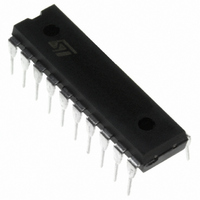
L4972A STMicroelectronics, L4972A Datasheet - Page 2

L4972A
Manufacturer Part Number
L4972A
Description
IC REG SW 2A 5.1V-40V 20-DIP
Manufacturer
STMicroelectronics
Type
Step-Down (Buck)r
Datasheet
1.L4972AD013TR.pdf
(22 pages)
Specifications of L4972A
Internal Switch(s)
Yes
Synchronous Rectifier
No
Number Of Outputs
1
Voltage - Output
5.1 ~ 40 V
Current - Output
2A
Frequency - Switching
100kHz
Voltage - Input
15 ~ 50 V
Operating Temperature
-40°C ~ 150°C
Mounting Type
Through Hole
Package / Case
20-DIP (0.300", 7.62mm)
Power - Output
5W
Output Voltage
50 V
Mounting Style
Through Hole
Input Voltage
50V
Output Current
2A
No. Of Outputs
1
Power Dissipation Pd
5W
No. Of Pins
20
Operating Temperature Range
-40°C To +150°C
Filter Terminals
Through Hole
Rohs Compliant
Yes
Lead Free Status / RoHS Status
Lead free / RoHS Compliant
Other names
497-6698-5
L4972A
L4972A
Available stocks
Company
Part Number
Manufacturer
Quantity
Price
Part Number:
L4972A
Manufacturer:
ST
Quantity:
20 000
Company:
Part Number:
L4972AD
Manufacturer:
STM
Quantity:
3 697
Part Number:
L4972AD
Manufacturer:
STM
Quantity:
20 000
Company:
Part Number:
L4972AD013TR
Manufacturer:
SII
Quantity:
4 466
Part Number:
L4972AD013TR
Manufacturer:
ST
Quantity:
20 000
L4972A
Table 2. Pin Description
Figure 3. Pin Connection (Top view)
2/22
5, 6 15,
12, 19
N°
16
10
11
13
14
17
18
20
1
2
3
4
7
8
9
FEEDBACK INPUT
SUPPLY VOLTAGE
COMPENSATION
RESET DELAY
RESET INPUT
FREQUENCY
BOOTSTRAP
OSCILLATOR
OSCILLATOR
SOFT START
SYNC INPUT
RESET OUT
GROUND
OUTPUT
V
N.C.
Pin
V
start
ref
FEEDBACK IN.
RESET DELAY
P. FAIL INPUT
FREQ. COMP.
SOFT START
BOOTSTRAP
SYNC INPUT
RESET OUT
A C
properly the internal D-MOS transistor.
A C
signal delay time.
Open Collector Reset/power Failand the output voltages are safe. Signal Output.
This output is high when the supply
Input of Power Fail Circuit. The threshold is 5.1V. It may be connected via a divider
to the input for power fail function. It must be connected to the pin 14 an external
30KΩ resistor when power fail signal not required.
Common Ground Terminal
A series RC network connected between this terminal and ground determines the
regulation loop gain characteristics.
Soft Start Time Constant. A capacitor is connected between the sterminal and
ground to define the soft start time constant.
The Feedback Terminal of the Regulation Loop. The output is connected directly to
this terminal for 5.1V operation; It is connected via a divider for higher voltages.
Multiple L4972A’s are synchronized by connecting pin 10 inputs together or via an
external syncr. pulse.
Unregulated Input Voltage.
Not Connected.
5.1V V
Internal Start-up Circuit to Drive the Power Stage.
R
current of C
C
frequency.
Regulator Output.
osc
osc
boot
d
. External resistor connected to ground determines the constant charging
. External capacitor connected to ground determines (with R
capacitor connected between this terminal and ground determines the reset
GND
GND
ref
capacitor connected between this terminal and the output allows to drive
Device Reference Voltage.
osc
.
1
2
3
4
5
6
7
8
9
10
DIP20
20
19
18
17
16
15
14
13
12
11
Function
OUTPUT
N.C.
C OSC
R OSC
GND
GND
Vstart
Vref
N.C.
Vi
osc
) the switching


