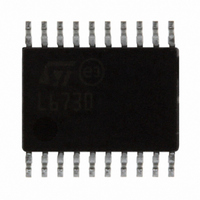
L6730TR STMicroelectronics, L6730TR Datasheet - Page 10

L6730TR
Manufacturer Part Number
L6730TR
Description
IC CTRLR ADJ STEP DOWN 20-TSSOP
Manufacturer
STMicroelectronics
Type
Step-Down (Buck)r
Datasheet
1.L6730TR.pdf
(52 pages)
Specifications of L6730TR
Internal Switch(s)
No
Synchronous Rectifier
Yes
Number Of Outputs
1
Voltage - Output
Adj to 0.6V
Frequency - Switching
100kHz ~ 1MHz
Voltage - Input
1.8 ~ 14 V
Operating Temperature
-40°C ~ 85°C
Mounting Type
Surface Mount
Package / Case
20-TSSOP Exposed Pad, 20-eTSSOP, 20-HTSSOP
Output Voltage
0.6 V
Input Voltage
1.8 V to 14 V
Maximum Operating Temperature
+ 85 C
Minimum Operating Temperature
- 40 C
For Use With
497-5868 - EVAL BOARD 30A 400KHZ L6730497-5501 - EVAL BOARD FOR L6730XX
Lead Free Status / RoHS Status
Lead free / RoHS Compliant
Current - Output
-
Power - Output
-
Lead Free Status / Rohs Status
Lead free / RoHS Compliant
Other names
497-5098-2
Available stocks
Company
Part Number
Manufacturer
Quantity
Price
Part Number:
L6730TR
Manufacturer:
ST
Quantity:
20 000
Pin connections and functions
10/52
Table 4.
Pin n.
11
12
13
14
15
16
17
18
19
20
-
Thermal PAD
PGOOD
PHASE
HGATE
LGATE
V
PGND
Name
BOOT
Pin connection (continued)
OCH
OCL
V
CCDR
CC
A resistor connected from this pin to ground sets the valley- current-limit.
The valley current is sensed through the low-side MOSFET(s). The
internal current generator sources a current of 100μA (I
to ground through the external resistor (R
is given by the following equation:
Connecting a capacitor from this pin to GND helps in reducing the noise
injected from V
high-frequency noise related to the GND. Connect a capacitor only to a
“clean” GND.
A resistor connected from this pin and the high-side MOSFET(s) drain
sets the peak-current-limit. The peak current is sensed through the high-
side MOSFET(s). The internal 100μA current generator (I
current from the drain through the external resistor (R
current threshold is given by the following equation:
This pin is connected to the source of the high-side MOSFET(s) and
provides the return path for the high-side driver. This pin monitors the
drop across both the upper and lower MOSFET(s) for the current limit
together with OCH and OCL.
This pin is connected to the high-side MOSFET(s) gate.
The high-side driver is supplied through this pin. Connect a capacitor from
this pin to the PHASE pin, and a diode from V
versus BOOT).
This pin has to be connected closely to the low-side MOSFET(s) source
in order to reduce the noise injection into the device. Connect to the PCB
power ground plane.
This pin is connected to the low-side MOSFET(s) gate.
5V internally regulated voltage. It is used to supply the internal drivers
and as a voltage reference. Filter it to GND with at least a 1µF ceramic
cap.
Supply voltage pin. The operative supply voltage range is from 4.5V to
14V.
This pin is an open collector output and it is pulled low if the output
voltage is not within the specified thresholds (90%-110%). If not used it
may be left floating. Pull up this pin to V
a logical signal.
Thermal Pad connects the silicon substrate and makes good thermal
contact with the PCB. Connect to the PCB power ground plane.
Doc ID 11938 Rev 3
CC
to the device, but can be a low impedance path for the
I
VALLEY
I
PEAK
Description
=
=
I
OCH
I
R
2
OCL
DSonHS
⋅
R
CCDR
DSonLS
⋅
OCL
R
⋅
R
OCH
OCL
). The over-current threshold
with a 10K resistor to obtain
CCDR
to this pin (cathode
OCH
OCL
L6730 - L6730B
OCH
). The over-
) from this pin
) sinks a


