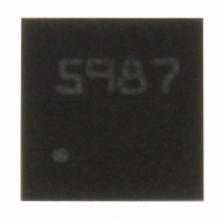
L5987TR STMicroelectronics, L5987TR Datasheet - Page 30

L5987TR
Manufacturer Part Number
L5987TR
Description
IC REG SW 3A STEPDOWN 8-VFQFPN
Manufacturer
STMicroelectronics
Type
Step-Down (Buck)r
Datasheet
1.L5987TR.pdf
(41 pages)
Specifications of L5987TR
Internal Switch(s)
Yes
Synchronous Rectifier
No
Number Of Outputs
1
Voltage - Output
0.6 ~ 18 V
Current - Output
3A
Frequency - Switching
250kHz
Voltage - Input
2.9 ~ 18 V
Operating Temperature
-40°C ~ 150°C
Mounting Type
Surface Mount
Package / Case
8-VFQFN, 8-VFQFPN
Power - Output
1.5W
Output Voltage
0.6 V
Output Current
3 A
Output Power
1.5 W
Input Voltage
2.9 V to 18 V
Switching Frequency
250 KHz
Mounting Style
SMD/SMT
Duty Cycle (max)
100 %
For Use With
497-8369 - BOARD EVALUATION FOR L5987
Lead Free Status / RoHS Status
Lead free / RoHS Compliant
Other names
497-8494-2
Available stocks
Company
Part Number
Manufacturer
Quantity
Price
Application information
6.6
30/41
of heat. The Rth
paragraph is about 60 °C/W for the VFQFPN package and about 40 °C/W for the HSOP
package.
Figure 17. Switching losses
Layout considerations
The PC board layout of switching DC/DC regulator is very important to minimize the noise
injected in high impedance nodes and interferences generated by the high switching current
loops.
In a step-down converter the input loop (including the input capacitor, the power MOSFET
and the free wheeling diode) is the most critical one. This is due to the fact that the high
value pulsed current are flowing through it. In order to minimize the EMI, this loop has to be
as short as possible.
The feedback pin (FB) connection to external resistor divider is a high impedance node, so
the interferences can be minimized placing the routing of feedback node as far as possible
from the high current paths. To reduce the pick up noise the resistor divider has to be placed
very close to the device.
To filter the high frequency noise, a small capacitor (220 nF) can be added as close as
possible to the input voltage pin of the device.
Thanks to the exposed pad of the device, the ground plane helps to reduce the thermal
resistance junction to ambient; so a large ground plane enhances the thermal performance
of the converter allowing high power conversion.
In
Figure 18
a layout example is shown.
JA
measured on the demonstration board described in the following
Doc ID 14972 Rev 3
L5987


