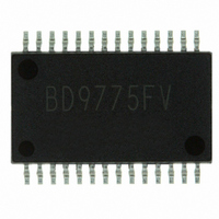
BD9775FV-E2 Rohm Semiconductor, BD9775FV-E2 Datasheet - Page 20

BD9775FV-E2
Manufacturer Part Number
BD9775FV-E2
Description
IC REG SW STEP DOWN HE 28-SSOP
Manufacturer
Rohm Semiconductor
Type
Step-Down (Buck)r
Specifications of BD9775FV-E2
Internal Switch(s)
No
Synchronous Rectifier
Yes
Number Of Outputs
2
Current - Output
400mA
Frequency - Switching
100kHz
Voltage - Input
6 ~ 30 V
Operating Temperature
-40°C ~ 85°C
Mounting Type
Surface Mount
Package / Case
28-SSOP
Power - Output
640mW
Mounting Style
SMD/SMT
Lead Free Status / RoHS Status
Lead free / RoHS Compliant
Voltage - Output
-
Lead Free Status / Rohs Status
Lead free / RoHS Compliant
Other names
BD9775FV-E2TR
● Pin Description
(BD9775FV)
●Block Diagram (BD9775FV)
●FUNCTION EXPLANATION (BD9775FV)
1.DC/DC Converter
・Reference Voltage
・Internal Regulator A (VREGA)
Stable voltage of compensated temperature, is generated from the power supply voltage (VCC). The reference voltage is 3.0V,
the accuracy is ±1%. Place a capacitor with low ESR (several decades mΩ) between VREF and GND.
5V is generated the power supply voltage. The voltage is for the driver of the synchronous rectification’s MOSFET. Place a
capacitor with low ESR (several decades mΩ) between VREGA and PGND.
10
11
12
13
14
1
2
3
4
5
6
7
8
9
DTC2
FB1
INV1
VREF
CTL1
CTL2
VCC
GND
DTC1
RT
CT
Fin
INV2
FB2
Fig.1
VREGA
VREGB
OUT2H
PVCC2
PVCC1
OUT2L
PGND
SYNC
OUT1
CL2
VS2
SCP
VS1
CL1
28
27
26
25
24
23
22
21
20
19
18
17
16
15
20/29
●PinNo/PinName (BD9775FV)
No.
Pin
10
12
13
14
15
16
17
18
19
20
21
22
23
24
25
26
27
28
11
1
2
3
4
5
6
7
8
9
VREGA
VREGB
PVCC2
OUT2H
PVCC1
OUT2L
PGND
SYNC
Name
VREF
DTC1
DTC2
OUT1
CTL1
CTL2
INV1
GND
INV2
VCC
SCP
VS2
VS1
FB1
FB2
CL2
CL1
FIN
Pin
RT
CT
Error amplifier output pin(Channel 1)
Error amplifier negative input pin(Channel 1)
Oscillator frequency adjustment pin
connected resistor
Oscillator frequency adjustment pin
connected capacitor
Oscillator synchronization pulse signal input pin
Low-noise ground
Reference voltage output pin
Maximum duty and soft start adjustment
pin(Channel 1)
Maximum duty and soft start adjustment
pin(Channel 2)
Error amplifier negative input pin(Channel 2)
Error amplifier output pin(Channel 2)
Enable/stand-by control input(Channel 1)
Enable/stand-by control input(Channel 2)
Main power supply pin
Synchronous rectification timing adjustable pin
Power ground (connected low-side gate driver
and digital ground)
Low-side ( synchronous rectifier ) gate driver
output pin(Channel 2)
Connected capacitor for internal regulator
Delay time of short circuit protection adjustment
pin connected capacitor
Over current detection voltage monitor pin
(connected FET drain, Channel 2)
Over current detection voltage adjustment pin
connected capacitor and resistor(Channel 2)
High-side gate driver power supply
input(Channel 2)
High-side gate driver output pin(Channel 2)
Connected capacitor for internal regulator
High-side gate driver output pin(Channel 1)
High-side gate driver power supply
input(Channel 1)
Over current detection voltage adjustment pin
connected capacitor and resistor(Channel 1)
Over current detection voltage monitor pin
(connected FET drain, Channel 1)
Description


