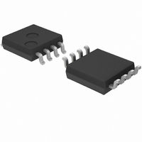
BD9850FVM-TR Rohm Semiconductor, BD9850FVM-TR Datasheet - Page 14

BD9850FVM-TR
Manufacturer Part Number
BD9850FVM-TR
Description
IC REG SW STEP DOWN HI EFF 8MSOP
Manufacturer
Rohm Semiconductor
Type
Step-Down (Buck)r
Series
-r
Datasheet
1.BD9850FVM-TR.pdf
(17 pages)
Specifications of BD9850FVM-TR
Internal Switch(s)
No
Synchronous Rectifier
No
Number Of Outputs
1
Current - Output
200mA
Frequency - Switching
100kHz ~ 2MHz
Voltage - Input
4 ~ 9 V
Operating Temperature
-40°C ~ 85°C
Mounting Type
Surface Mount
Package / Case
8-MSOP, Micro8™, 8-uMAX, 8-uSOP,
Power - Output
587mW
Mounting Style
SMD/SMT
Pwm Type
Controller
Frequency - Max
2MHz
Duty Cycle
-
Voltage - Supply
4 V ~ 9 V
Buck
Yes
Boost
No
Flyback
No
Inverting
No
Doubler
No
Divider
No
Cuk
No
Isolated
No
Lead Free Status / RoHS Status
Lead free / RoHS Compliant
Voltage - Output
-
Lead Free Status / Rohs Status
Lead free / RoHS Compliant
Available stocks
Company
Part Number
Manufacturer
Quantity
Price
Company:
Part Number:
BD9850FVM-TR
Manufacturer:
ST
Quantity:
110
Part Number:
BD9850FVM-TR
Manufacturer:
ROHM/罗姆
Quantity:
20 000
10)
8)
9)
IC pin input
This monolithic IC contains P+ isolation and P substrate layers between adjacent elements to keep them isolated. Pin junctions are formed at the
intersection of these P layers with the N layers of other elements, creating a parasitic diode or transistor. For example, the relation between each
potential is as follows:
Parasitic diodes can occur inevitably in the structure of the IC. The operation of parasitic diodes can result in mutual interference among circuits,
operational faults, or physical damage. Accordingly, methods by which parasitic diodes operate, such as applying a voltage that is lower than the
GND (P substrate) voltage to an input pin, should not be used.
Common impedance
The power supply and ground lines must be as short and thick as possible to reduce line impedance. Fluctuating voltage
line may damage the device.
On the application shown below, Vcc is short-circuited to the Ground with external diode charged, internal circuits may be damaged.
recommended to insert a backflow prevention diode in series with the Vcc or a bypass diode between each pin and Vcc.
When GND > Pin A and GND > Pin B, the Pin junction operates as a parasitic diode.
When Pin B > GND > Pin A, the PñN junction operates as a parasitic transistor.
(Pin A)
Player
N
(Pin A)
P +
GND
Resistor
Fig. 28 Typical simple construction of monolithic IC
N
Backflow prevention diode
Parasitic element
GND
P
Parasitic element
Bypass diode
P +
N
Fig. 29
14/16
Other proximity element
Vcc
(Pin B)
N
Parasitic element
(Pin B)
Output pin
P +
C
Transistor
B
B
E
N
N
(NPN)
GND
P
C
E
GND
Parasitic element
P +
Player
N
on the power ground
GND


