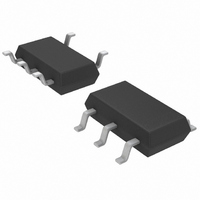
LTC3406BES5#TRMPBF Linear Technology, LTC3406BES5#TRMPBF Datasheet - Page 7

LTC3406BES5#TRMPBF
Manufacturer Part Number
LTC3406BES5#TRMPBF
Description
IC RG ST-DWN SYNC 600MA TSOT23-5
Manufacturer
Linear Technology
Type
Step-Down (Buck)r
Datasheet
1.LTC3406BES5TRMPBF.pdf
(16 pages)
Specifications of LTC3406BES5#TRMPBF
Internal Switch(s)
Yes
Synchronous Rectifier
Yes
Number Of Outputs
1
Voltage - Output
0.6 ~ 5.5 V
Current - Output
600mA
Frequency - Switching
1.5MHz
Voltage - Input
2.5 ~ 5.5 V
Operating Temperature
-40°C ~ 85°C
Mounting Type
Surface Mount
Package / Case
TSOT-23-5, TSOT-5, TSOP-5
Lead Free Status / RoHS Status
Lead free / RoHS Compliant
Power - Output
-
Other names
LTC3406BES5#TRMPBFTR
Available stocks
Company
Part Number
Manufacturer
Quantity
Price
Dropout Operation
As the input supply voltage decreases to a value approach-
ing the output voltage, the duty cycle increases toward the
maximum on-time. Further reduction of the supply voltage
forces the main switch to remain on for more than one cycle
until it reaches 100% duty cycle. The output voltage will then
be determined by the input voltage minus the voltage drop
across the P-channel MOSFET and the inductor.
An important detail to remember is that at low input supply
voltages, the R
(see Typical Performance Characteristics). Therefore, the
user should calculate the power dissipation when the
LTC3406B is used at 100% duty cycle with low input
voltage (See Thermal Considerations in the Applications
Information section).
Low Supply Operation
The LTC3406B will operate with input supply voltages as
low as 2.5V, but the maximum allowable output current is
reduced at this low voltage. Figure 2 shows the reduction
in the maximum output current as a function of input
voltage for various output voltages.
OPERATIO
DS(ON)
U
(Refer to Functional Diagram)
of the P-channel switch increases
Slope Compensation and Inductor Peak Current
Slope compensation provides stability in constant fre-
quency architectures by preventing subharmonic oscilla-
tions at high duty cycles. It is accomplished internally by
adding a compensating ramp to the inductor current
signal at duty cycles in excess of 40%. Normally, this
results in a reduction of maximum inductor peak current
for duty cycles > 40%. However, the LTC3406B uses a
patent-pending scheme that counteracts this compensat-
ing ramp, which allows the maximum inductor peak
current to remain unaffected throughout all duty cycles.
Figure 2. Maximum Output Current vs Input Voltage
1200
1000
800
600
400
200
0
2.5
V
V
OUT
OUT
3.0
= 1.8V
= 1.5V
SUPPLY VOLTAGE (V)
3.5
V
OUT
4.0
= 2.5V
4.5
5.0
3406B F02
LTC3406B
5.5
3406bfa
7


