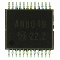
AN8049SH-E1 Panasonic - SSG, AN8049SH-E1 Datasheet - Page 22

AN8049SH-E1
Manufacturer Part Number
AN8049SH-E1
Description
IC MULTI CONFIG 40MA SSOP24D
Manufacturer
Panasonic - SSG
Type
Step-Down (Buck), Step-Up (Boost), Invertingr
Specifications of AN8049SH-E1
Internal Switch(s)
Yes
Synchronous Rectifier
No
Number Of Outputs
3
Current - Output
40mA
Frequency - Switching
20kHz ~ 1MHz
Voltage - Input
1.8 ~ 14 V
Operating Temperature
-30°C ~ 85°C
Mounting Type
Surface Mount
Package / Case
24-SSOP
Power - Output
146mW
Lead Free Status / RoHS Status
Contains lead / RoHS non-compliant
Voltage - Output
-
Other names
AN8049SHE1
AN8049SHE1TR
AN8049SHE1TR
Available stocks
Company
Part Number
Manufacturer
Quantity
Price
Company:
Part Number:
AN8049SH-E1V
Manufacturer:
MITSUMI
Quantity:
2 511
Part Number:
AN8049SH-E1V
Manufacturer:
PANASONIC/松下
Quantity:
20 000
AN8049SH
I Application Notes (continued)
22
R
[10] Notes on power supply printed circuit board design
T
low noise and high efficiency.
1. Use extremely wide lines for the ground lines, and isolate the IC ground from the power system ground.
2. Position input filter capacitors as close as possible to the V
3. Keep the length of the line between the OUT pin and the switching device as short as possible to provide a clean
4. Use longer lines for the low-impedance side of the output voltage detection resistors.
1) Use a ground line separate from the power system ground for the capacitor and resistor connected to the OSC
2) Lower the OSC pin impedance by either decreasing the value of the resistor R
Careful attention must be paid to the following points when designing the printed circuit board layout to achieve
In particular, during light-load operation (when the on-duty is low) switching noise can enter the system at the lower
limit of the sawtooth waveform causing the operating frequency to vary every period and resulting in unstable
control.
Take measures described as 1) and 2) below, and assure that switching noise does not appear on the sawtooth
waveform.
(See the figures below.)
If switching noise cannot be suppressed even with exceptionally large capacitors, or if there are limitations on the
size of capacitors that can be used, install an CR filter in the input to reduce switching noise. Problems may occur
if switching noise enters the IC by any route.
switching waveform to the switching device.
pin.
capacitor C
C
T
(2) Modify the
values of the
capacitor and
resistor.
Q1
T
.
Common impedance
V
IN
R
T
(1) Use separate lines.
C
T
V
GND
OUT
Lower limit voltage
of the sawtooth wave
during stable operation
Q1
V
SDH00012BEB
IN
CC
V
GND
and ground pins.
OUT
The frequency changes at each period.
Small
T
or increasing the value of the
Noise is picked up
and the IC switches
from charge to
discharge operation.
Large


