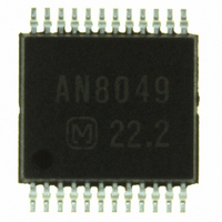
AN8049SH-E1 Panasonic - SSG, AN8049SH-E1 Datasheet - Page 11

AN8049SH-E1
Manufacturer Part Number
AN8049SH-E1
Description
IC MULTI CONFIG 40MA SSOP24D
Manufacturer
Panasonic - SSG
Type
Step-Down (Buck), Step-Up (Boost), Invertingr
Specifications of AN8049SH-E1
Internal Switch(s)
Yes
Synchronous Rectifier
No
Number Of Outputs
3
Current - Output
40mA
Frequency - Switching
20kHz ~ 1MHz
Voltage - Input
1.8 ~ 14 V
Operating Temperature
-30°C ~ 85°C
Mounting Type
Surface Mount
Package / Case
24-SSOP
Power - Output
146mW
Lead Free Status / RoHS Status
Contains lead / RoHS non-compliant
Voltage - Output
-
Other names
AN8049SHE1
AN8049SHE1TR
AN8049SHE1TR
Available stocks
Company
Part Number
Manufacturer
Quantity
Price
Company:
Part Number:
AN8049SH-E1V
Manufacturer:
MITSUMI
Quantity:
2 511
Part Number:
AN8049SH-E1V
Manufacturer:
PANASONIC/松下
Quantity:
20 000
I Usage Notes
[1] Allowable power dissipation
[2] Allowable V
1. Since the power dissipation (P) in this IC increases proportionally with the supply voltage, applications must be careful
2. If the IC is shorted to ground, shorted to V
biased by V
output is shorted.
ripple filter in the V
as close to the IC as possible.
may differ depending on the actual system of the power supply circuit. Also note that this allowable range is a design
target, and is not guaranteed by testing of all samples.
to operate so that the loss does not exceed the allowable power dissipation, P
components will be destroyed.
V
The figure shows the allowable range for V
Note that the allowable range shown here is the result of testing the IC independently, and that the allowable range
CC
Reference formula:
P = (V
ripple due to the switching transistor being turned on and off can cause this IC's U.V.L.O. circuit, which is
< P
CC
V
I
Du
V
I
Du
V
I
Du
I
SO(OUT)1
SO(OUT)2
OUT3
CC
D
BEQ1
BEQ2
O(SAT)3
, to operate incorrectly, and can cause the S.C.P. capacitor charging operation to fail to start when the
CC
1
2
3
CC
−V
ripple
CC
BEQ1
: The voltage between the base and emitter of the channel 1 npn transistor
: The OUT1 pin output source current
: The output 1 on-duty
: The voltage between the base and emitter of the channel 2 npn transistor
: The OUT2 pin output source current
: The output 2 on-duty
: The OUT3 pin saturation voltage (0.5 V maximum when I
: The OUT3 pin current (This will be {V
: The output 3 on-duty
: The V
(This is set by the resistor connected to the RB1 pin. When R
maximum.)
(This is set by the resistor connected to the RB2 pin. When R
maximum.)
line or by inserting a capacitor between the IC GND and V
) × I
100k
10M
10k
1M
CC
0
SO(OUT)1
pin current
1
× Du
Allowable range
when V
V
1
2
CC
+ (V
ripple voltage V
Allowable V
CC
CC
is 3 V.
CC
CC
3
ripple. Applications should reduce V
SDH00012BEB
− V
, or inserted incorrectly, either the device itself or peripheral
Allowable range
when V
BEQ2
4
CC
CC
CC
) × I
is 10 V.
(AC) (V[p-p])
ripple
CC
5
SO(OUT)2
− V
BEQ3
6
× Du
− V
D
7
, for the package. See the P
2
O(SAT)3
+ V
OUT3
CC
B
B
O(SAT)3
is 1 kΩ, I
is 1 kΩ, I
8
}/R
pins and locating that capacitor
is 40 mA.)
CC
O3
× I
ripple either by inserting a
.)
OUT3
SO(OUT)1
SO(OUT)2
× Du
AN8049SH
will be 34 mA,
will be 34 mA,
D
3
+ V
T
CC
a
curve.
× I
11
CC


