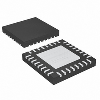
MAX1531ETJ+ Maxim Integrated Products, MAX1531ETJ+ Datasheet - Page 31

MAX1531ETJ+
Manufacturer Part Number
MAX1531ETJ+
Description
IC PS CTRLR MULTI-OUTPUT 32TQFN
Manufacturer
Maxim Integrated Products
Datasheet
1.MAX1531ETJT.pdf
(33 pages)
Specifications of MAX1531ETJ+
Applications
Five Power Supply Monitor
Voltage - Supply
4.5 V ~ 28 V
Current - Supply
1.7mA
Operating Temperature
-40°C ~ 85°C
Mounting Type
Surface Mount
Package / Case
32-TQFN Exposed Pad
Voltage - Output
1.25 ~ 16.5 V
Number Of Outputs
5
Lead Free Status / RoHS Status
Lead free / RoHS Compliant
Voltage - Input
-
Lead Free Status / Rohs Status
Details
4) Next, calculate the pole set by each linear regula-
5) Next, calculate the zero caused by the output
6) To ensure stability, choose C
Careful PC board layout is important for proper opera-
tion. Use the following guidelines for good PC board
layout:
1) Place the high-power components of the step-down
2) Create islands for the analog ground (AGND),
tor’s feedback resistance and the capacitance
(C
5pF including stray capacitance):
capacitor’s ESR:
where R
the crossover occurs well before the poles and zero
calculated in steps 2) to 5). The poles in steps 3)
and 4) generally occur at several megahertz and
using ceramic capacitors ensures the ESR zero
occurs at several megahertz as well. Placing the
crossover below 500kHz is sufficient to avoid the
amplifier-delay pole and generally works well, unless
unusual component choices or extra capacitances
move the other poles or zero below 1MHz.
regulator (input capacitors, MOSFETs, inductor,
and output capacitors) first, with any grounded
connections adjacent. Connect these components
with short, wide traces. Avoid using vias in the
high-current paths. If vias are unavoidable, use
many vias in parallel to reduce resistance and
inductance.
power ground (PGND), and individual linear regula-
tor grounds. Connect all these ground areas
FBL_
Multiple-Output Power-Supply Controllers for
) between FBL_ and AGND (approximately
ESR
f
f
f
f
f
POLE FBL
POLE FBL
POLE FBL
POLE FBL
POLE FBL
PC Board Layout and Grounding
f
ESR ZERO
is the equivalent series resistance of C
(
(
(
(
(
______________________________________________________________________________________
_
1
2
3
4
5
)
)
)
)
)
=
=
=
=
=
2
2
2
2
2
π
=
π
π
π
π
C
C
C
C
C
2π
FBL
FBL
FBL
FBL
FBL
C R
LR ESR
LR
1
2
3
4
5
1
(
1
R
(
(
(
1
(
1
1
1
R
R
R
R
9
large enough so that
18
25
28
22
||
R
||
||
||
||
10
R
R
R
R
19
26
29
)
23
)
)
)
)
and
LR
.
3) Place the IN pin and VL pin bypass capacitors
4) Since both MOSFETs are used for current sensing,
5) Place all feedback voltage-divider resistors as
6) Minimize the length and maximize the width of the
7) Minimize the size of the LX node while keeping it
(islands) together at only one location, which is a
via connected to the backside pad of the device.
All voltage-feedback dividers should be connected
to the analog ground island. The step-down regula-
tor’s input and output capacitors, and the charge
pump components should be a wide power ground
plane. The power ground plane should be connect-
ed to the power ground pin (PGND) with a wide
trace. Maximizing the width of the power ground
traces improves efficiency, and reduces output
voltage ripple and noise spikes. All other ground
connections, such as the VL and IN pin bypass
capacitor and the linear regulator output capaci-
tors, should be star-connected to the backside of
the device with wide traces. Make no other connec-
tions between these separate ground planes.
within 5mm from the IC and connect them to their
respective pins with short, direct connections.
care must be taken to ensure that noise and DC
errors do not corrupt the sense signals. Place both
MOSFETs close to the IC. Connect PGND to the
source of the low-side MOSFET with a short, wide
trace. Connect DL to the gate of the low-side MOS-
FET with a short, wide trace. Ensure that the traces
from DL to low-side MOSFET to PGND total no
more than 50 squares. Connect LX close to the
connection point between the low-side and high-
side MOSFETs with a short, wide trace. Connect
DH to the gate of the high-side MOSFET with a
short, wide trace. Ensure that the traces from DH to
high-side MOSFET to LX total no more than 50
squares (50 squares corresponds to 20 mils wide if
the total trace is 1in long).
close to their respective feedback pins as possible.
The divider’s center trace should be kept short.
Placing the resistors far away causes their FB
traces to become antennas that can pick up
switching noise. Care should be taken to avoid run-
ning any feedback trace near LX or the switching
nodes in the charge pumps.
traces between the output capacitors and the load
for best transient responses.
wide and short. Keep the LX node away from feed-
back nodes and analog ground. Use DC traces as
shield if necessary.
LCD Monitors
31


