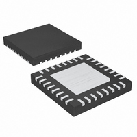
MAX1531ETJ+ Maxim Integrated Products, MAX1531ETJ+ Datasheet - Page 29

MAX1531ETJ+
Manufacturer Part Number
MAX1531ETJ+
Description
IC PS CTRLR MULTI-OUTPUT 32TQFN
Manufacturer
Maxim Integrated Products
Datasheet
1.MAX1531ETJT.pdf
(33 pages)
Specifications of MAX1531ETJ+
Applications
Five Power Supply Monitor
Voltage - Supply
4.5 V ~ 28 V
Current - Supply
1.7mA
Operating Temperature
-40°C ~ 85°C
Mounting Type
Surface Mount
Package / Case
32-TQFN Exposed Pad
Voltage - Output
1.25 ~ 16.5 V
Number Of Outputs
5
Lead Free Status / RoHS Status
Lead free / RoHS Compliant
Voltage - Input
-
Lead Free Status / Rohs Status
Details
Increasing the flying capacitor value lowers the effec-
tive source impedance and increases the output cur-
rent capability. Increasing the capacitance indefinitely
has a negligible effect on output current capability
because the internal switch resistance and the diode
impedance place a lower limit on the source imped-
ance. A 0.1µF ceramic capacitor works well in most
low-current applications. The voltage rating for a given
flying capacitor (CX) must exceed the following:
where N is the stage number in which the flying capaci-
tor appears, and V
down regulator.
Increasing the output capacitance or decreasing the
ESR reduces the charge pump output ripple voltage
and the peak-to-peak transient voltage. With ceramic
capacitors, the output voltage ripple is dominated by
the capacitance value. Use the following equation to
approximate the required capacitor value:
where V
ripple.
Use low-cost silicon switching diodes with a current rat-
ing equal to or greater than 2 times the average
charge-pump input current. If it helps avoid an extra
stage, some or all of the diodes can be replaced with
Schottky diodes with an equivalent current rating.
Adjust the positive linear regulator (LR1 to LR4) output
voltages by connecting a resistive voltage-divider from
the output to AGND with the center tap connected to
FBL_ (Figure 1). Select the lower resistor of the divider
in the 10kΩ to 30kΩ range. Calculate the upper resistor
with the following equation:
where V
Adjust the negative linear regulator (LR5) output volt-
age by connecting a resistive voltage-divider from
R
Multiple-Output Power-Supply Controllers for
FBL
UPPER
RIPPLE
_ is 1.238V (typ).
=
is the peak-to-peak value of the output
C
R
OUT
LOWER
______________________________________________________________________________________
Linear Regulator Controllers
IN
V
Charge-Pump Output Capacitors
CX
≥
is the input voltage of the step-
Charge-Pump Rectifier Diodes
2
> N x V
f
×
OSC RIPPLE
[
(
I
V
LOAD
Output Voltage Selection
OUT
V
IN
_
/
V
Flying Capacitors
FBL
_
)
−
1
]
V
(Figure 1). Select R29 in the 10kΩ to 30kΩ range.
Calculate R28 with the following equation:
where V
The pass transistor must meet specifications for DC
current gain (h
and power dissipation. The transistor’s current gain lim-
its the guaranteed maximum output current to:
where I
rent, V
tor, and R
the transistor’s base and emitter. Furthermore, the tran-
sistor’s current gain increases the linear regulator’s DC
loop gain (see the Stability Requirements section),
which may destabilize the output. Therefore, transistors
with current gain over 300 at the maximum output cur-
rent can be difficult to stabilize and are not recom-
mended unless the high gain is needed to meet the
load current requirements.
The transistor’s saturation voltage at the maximum out-
put current determines the minimum input-to-output
voltage differential that the linear regulator supports.
Also, the package’s power dissipation limits the usable
maximum input-to-output voltage differential. The maxi-
mum power dissipation capability of the transistor’s
package and mounting must exceed the actual power
dissipation in the device. The power dissipation equals
the maximum load current (I
mum input-to-output voltage differential:
where V
linear regulator, and V
linear regulator.
Ideally, the output voltage of a linear regulator should
not contain any ripple. In the MAX1530/MAX1531, the
step-down regulator’s switching noise can couple to
the linear regulators, creating output voltage ripple.
Following the PC board layout guidelines in the PC
Board Layout and Grounding section can significantly
reduce noise coupling. If there is still an unacceptable
GOFF
R
BE
DRV
28
to VL with the center tap connected to FBL5
FBL5
P I
LRIN(MAX)
is the base-emitter voltage of the pass transis-
=
BE
=
I
LOAD MAX
LOAD MAX
R
is the minimum guaranteed base drive cur-
= 125mV and V
29
is the pullup resistor connected between
FE
×
(
(
), collector-emitter saturation voltage,
[
(
is the maximum input voltage of the
V
FBL
)
)
LROUT
=
LCD Monitors
×
5
⎛
⎜
⎝
(
I
V
−
DRV
LRIN MAX
V
Pass Transistor Selection
GOFF
LOAD(MAX)
L
is the output voltage of the
−
= 5.0V.
(
R
Output Voltage Ripple
V
BE
BE
) /(
)
V
⎞
⎟ ×
⎠
−
L
V
−
) times the maxi-
h
LROUT
V
FE
FBL
5
)
)
]
29


