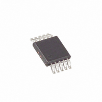
MAX1820XEUB+T Maxim Integrated Products, MAX1820XEUB+T Datasheet - Page 8

MAX1820XEUB+T
Manufacturer Part Number
MAX1820XEUB+T
Description
IC REG BUCK WCDMA 10-MSOP
Manufacturer
Maxim Integrated Products
Datasheet
1.MAX1821EUBT.pdf
(18 pages)
Specifications of MAX1820XEUB+T
Applications
Converter, WCDMA Power Amplifier Applications
Voltage - Input
2.6 ~ 5.5 V
Number Of Outputs
1
Voltage - Output
0.4 ~ 3.4 V
Operating Temperature
0°C ~ 85°C
Mounting Type
Surface Mount
Package / Case
10-MSOP, Micro10™, 10-uMAX, 10-uSOP
Lead Free Status / RoHS Status
Lead free / RoHS Compliant
WCDMA Cellular Phone 600mA
Buck Regulators
8
(T
MAX1820
A
UCSP
= +25°C, unless otherwise noted.)
_______________________________________________________________________________________
A1
A2
A3
MAX1820
µMAX
1
2
3
1.6
1.2
0.8
0.4
1.6
1.2
0.8
0.4
0
0
0.1
(V
0.1
(V
IN
IN
PIN
OUTPUT SWITCHING HARMONICS
OUTPUT SWITCHING HARMONICS
= 3.8V, V
= 4.2V, V
MAX1821
UCSP
A1
A2
—
vs. FREQUENCY
vs. FREQUENCY
FREQUENCY (MHz)
FREQUENCY (MHz)
OUT
OUT
= 3.4V, I
= 0.4V, I
1
1
MAX1821
µMAX
LOAD
—
LOAD
1
2
Typical Operating Characteristics (continued)
= 600mA)
= 30mA)
10
10
NAME
COMP
SKIP
OUT
PWM/Skip-Mode Input. Drive with logic 0 to use PWM at medium
and heavy loads and pulse skipping at light loads. Drive with
logic 1 to force PWM at all loads.
Compensation. Typically, connect an 82k (for MAX1821) or
43k (for MAX1820) series resistor and 330pF capacitor from
this pin to GND to stabilize the regulator.
Output Voltage Sense Input. Connect OUT directly to the output.
4.0
3.0
2.0
1.0
1.6
1.2
0.8
0.4
0
0
0.1
(V
0.1
IN
OUTPUT SWITCHING HARMONICS
= 3.8V, V
OUTPUT NOISE (V
V
OUT
1
= 1.8V, I
vs. FREQUENCY
FREQUENCY (MHz)
FREQUENCY (MHz)
OUT
= 1.8V, I
1
OUT
FUNCTION
10
IN
= 300mA)
= 3.6V,
LOAD
= 300mA)
100
Pin Description
250
10


